Simulation is essential to successful design of modern semiconductors

The application of lithography simulation has become mandatory for the research and development departments of semiconductor manufacturers and for many of their suppliers. Modern simulation software for lithography describes the light diffraction from the mask, the imaging of the mask by a high numerical aperture projection system, the interaction of the projected light with the photoresist, the chemical modifications of the photoresist during baking steps, and the chemical development of the resist.1 The models for the individual process steps are combined to create a general lithography simulator.
A typical simulation flow of a lithographic process is shown in Fig. 1. The mask layout is defined by a pattern of dark features on a bright background. Fourier transformation of the mask transmission generates the diffraction spectrum, which corresponds to the angular distribution of the diffracted light at the entrance pupil of the projection system.
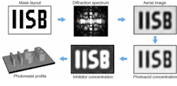
FIGURE 1. In a schematic presentation of the simulation steps of lithographic processes, bright areas of mask layout are transparent and dark areas are not. The width of the letter "I" is 250 nm. In the diffraction spectrum for λ = 248 nm, intensity goes from low/dark to high/white. The aerial image is shown at the best focus position: NA = 0.75, σ = 0.5. Photoacid concentration goes from low/dark to high/bright. Inhibitor concentration goes from low/dark to high/bright. Photoresist profile follows 60-s development.
The intensity distribution of the light in the image plane, the so-called aerial image, is obtained by inverse Fourier transformation and by an integration over the angular range that is used to illuminate the mask. The projected light, the aerial image, provides very useful information regarding the performance of a lithographic process. The basic structure of the letters, especially of lines or "I"s is clearly transferred by the projection system. However, some details of the mask layout such as the ends of lines (upper and lower part of the "I"s) and contact holes (inner parts of the "B") are blurred.
The lower part of Fig. 1 shows the status of the photoresist during the processing steps. In modern chemically amplified resists, the incident light generates a certain amount of photoacid in the exposed areas. Heating of the photoresist following post-exposure bake results in an acid-catalyzed decomposition of dissolution inhibitors. These inhibitors make the resist almost not dissolvable in the dark unexposed areas, whereas the light/acid-catalyzed decomposition renders the resist material dissolvable in the bright/exposed areas. The resulting shape of the resist after development can be observed in the lower left part of the figure.
Optimizing process parameters
Predictive lithography simulation models and software implementations can be used for the optimization of process parameters. Optical resolution-enhancement techniques that modify the layout of the mask—such as optical proximity correction (OPC) and phase- shift masks (PSM)—and the geometry of the illumination, such as off-axis illumination (OAI), are characterized by many free parameters. The optimization of the large number of mask and illumination options and parameters requires the application of robust and versatile optimization algorithms. Recently, the application of genetic algorithms for the optimization of mask and source geometries was proposed.2 The concept's potential was demonstrated by the automatic generation of mask layouts and illumination geometries for the patterning of simple features such as lines/spaces and contact holes.
Critical diffraction phenomena
Smaller features and more-complex mask and wafer geometries require the application of more-accurate modeling approaches. For standard chromium-on-glass masks with moderate feature sizes, the transmission of light through this mask is directly related to the mask design. In other words, the absolute value of the transmission is close to 0 in chromium-covered areas and 1 in the open areas. The accurate computation of light transmission to advanced masks with very small chromium features or phase-shift masks requires the application of rigorous electromagnetic-field solvers like finite-difference time-domain (FDTD) methods.3
Rigorous electromagnetic-field simulation is also necessary to explore wafer topography effects that can occur in certain situations (see Fig. 2). The geometry of the mask is given on the left-hand side of the figure. A 70-nm wide and 175-nm high poly-Si line parallel to the z-axis was generated in a previous lithography step. This poly-Si line is used as a mask for the following implantation steps. The wafer is coated with a 500-nm-thick deep-UV photoresist. The binary mask consists of 250-nm lines with a pitch of 1000 nm that are perpendicular to the poly-Si line. The exposures are performed with a krypton fluoride (KrF) laser-based stepper (λ = 193 nm).
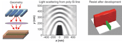
The central part of Fig. 2 shows the simulated intensity distribution perpendicular with respect to the poly-Si line at the center of a space. The light is diffracted away from the poly-Si line, resulting in a region close to the bottom of the poly-Si line with very small intensity of light. The resulting photoresist profile is shown in the right part of the figure. A pronounced footing of the resist at the bottom of the poly-Si line can be observed. This footing results from the reduced light intensity close to the bottom of the poly-Si line. Comparisons of similar simulations with experimental measurements and in-depth discussions of this footing effect have been published.4
References
- A. Erdmann and W. Henke, Proc. SPIE 3729: 480 (1999).
- A. Erdmann, R. Farkas, T. Fühner, B. Tollkühn, and G. Kókai "Mask and Source Optimization for Lithographic Imaging Systems," SPIE Annual Meeting, San Diego CA (August 2003).
- A. Erdmann and C. Friedrich, Proc. SPIE 4000: 684 (2000).
- A. Erdmann et al., Proc. SPIE 5040, 101 (2003).
ANDREAS ERDMANN, author of the TASPAL Maxwell solver in SOLID-CTM lithography simulation software and co-author of the SOLID-C lithography simulator, heads the lithography group at the Fraunhofer Institute of Integrated Systems and Device Technology Division (IISB), Schottkystrasse 10, 91058 Erlangen, Germany; e-mail: [email protected].