Design code models unconventional sources
Design code models unconventional sources
Flexible optical design software simulates the emission of a light-emitting diode, allowing designers to analyze performance of systems from the source to the detector.
Yan Cornil
Light-emitting diodes (LEDs) have widespread applications as indicator lights, liquid-crystal-display backlighting, or sources imaged or projected by optical systems. When LEDs are used as indicators or backlighting sources, their pattern of illumination is noncritical. If they are integrated into optical systems, however, accurate source modeling is critical if designers are to arrive at the best optical configuration. Solstis optical design software from Optis (Toulon, France) can simulate the output of an LED source, including focusing and diffusion effects from the epoxy dome and the photometric behavior of the emission chi¥itself.
Dome effects
The Temic (Nürnberg, Germany) light-emitting diode modeled here (TS1P520) generates 2.5 mW with a Gaussian spectral distribution ranging from 900 to 1000 nm. The dome is a standard epoxy casing 4.9 mm in diameter, with a 4.25 mm radius of curvature on the emission tip.
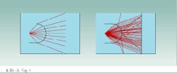
The curved surface of the epoxy dome acts as a lens to focus the chi¥emission for directional illumination. By treating the emission chi¥as a point source and the curved dome as a simple lens, we can perform a ray trace and model the geometrical effects of the epoxy (see Fig. 1, left).
We must also include the effects of diffraction to fully understand the LED output. The epoxy material of the dome diffuses the chi¥emission, leading to surface scatter and self-focusing effects. Using the Solstis diffusion module, we can characterize the process as a Lambertian function, simulating the form of the LED output for an assumed 10% flux attenuation caused by diffusion and scattering at the dome surface (see Fig. 1, right).
Emission chi¥simulation
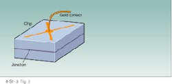
Light-emitting diodes produce an emission that is distinctly different from the point or extended sources that are the default sources in typical optical design code. As in many LEDs, the cross-shaped contact of the TS1P520 obscures segments of the chi¥output, creating a cruciform emission pattern (see Fig. 2). This effect can be minimized with the diffusion effects of the epoxy dome discussed earlier, but the cross pattern is still visible.
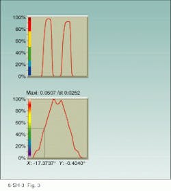
This LED output can be simulated in Solstis with the "User Defined Sources" option. To account for diffraction effects, the emission pattern must be modeled in the near- and far-field. In the near-field, the relative emittance is defined numerically over a 10 ¥ 10 array of points (see Fig. 3). Such in formation can be obtained from the manufacturer and entered into the program.
Performance in the far-field is likewise entered numerically as an array as large as 100 ¥ 100 points. In our example, the data obtained from a 20 ¥ 20 array is in agreement with the manufacturer`s model. The emittance pattern was determined by assuming a Lambertian intensity distribution and normalizing it to match that of the manufacturer`s data sheet.
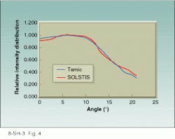
The program allows us to model the spectral character of the LED as a Gaussian distribution with an automatic definition. This spectral range is numerically defined by a maximum of 100 points; we used 20 points in this example. We restated the 25-mW ouput power in terms of intensity as 50 mW/sr and used this value to scale the emission power in the simulation. A comparison of the simulated intensity pattern and the manufacturer`s information shows that the software model is in agreement with the experimental data (see Fig. 4).
It is important to note that only generally accessible information from the manufacturer`s data sheet has been used to simulate this source, and the method can be applied to LEDs operating at any wavelength. The de signer can now model and analyze the global optical system from the source u¥to detector. o
FIGURE 1. Optical design program models the focusing (left) and diffusion (right) effects of the light-emitting-diode epoxy dome on the emission pattern of the chip.
FIGURE 2. Cruciform contact on light-emitting diode (left) causes a cross-shaped shadow in the emission pattern of the device (right).
FIGURE 3. Near-field (top) and far-field (bottom) emission patterns modeled by Solstis show good agreement with manufacturer`s data for the TS1P520 light-emitting diode.
FIGURE 4. Comparison of light-emitting-diode intensity distribution as simulated by Solstis closely conforms to manufacturer`s model.


