MICROELECTRONICS PROCESSING: Software reveals interaction of light with matter

Models that simulate the interaction of light with matter are valuable to researchers and engineers in the semiconductor industry. Light is used at several steps in the manufacture of an integrated-circuit chip (IC), for example, in wafer and chip marking, lithographic patterning, defect detection, and memory repair. For some of these steps, a software model is essential to the detailed understanding of the light-based interaction itself. If the model is accurate enough, it can also serve as an aid in the design of optical, mechanical, and electronic hardware required for the production of ICs. Of course, it is empirical testing that determines whether or not a software model is adequate.
Optics and chemistry
In projection microlithography, a semiconductor wafer coated with photoresist is exposed to a light pattern formed by a lens. The wafer is then washed in a developer solution, at which point either the exposed portion of the resist is removed (positive resist) or the unexposed portion is removed (negative resist). After etching and the addition of another process layer, the wafer is recoated with resist and the procedure repeated until all required IC layers are in place.
Microlithography can produce features in resist that are smaller than the wavelength of the exposure light. This is a result not just of the high resolution of the projection lens but also of the way resist responds to light. Because the developing process must result either in an area cleared of resist or an area still covered with resist, a threshold is added to the patterning process. Although this effect can improve resolution, it also prevents the designer of a lithographic lens from using the image-analysis output from a lens-design program in itself as a model for final performance of the system.
Other resist properties complicate analysis further. A layer of resist has a finite thickness, within which light reflected from the wafer can interfere with direct light to create standing waves, resulting in internal planes of greater or less exposure. The light-absorption coefficient varies from one resist to the next. Variations in pre- or postexposure baking of the resist—necessary steps in the lithographic process—can affect resolution and linewidth. The projection lens itself has aberrations that affect image quality in unusual ways due to the nonlinear response of resist. Thus, software that models lithographic imaging must take into account the chemistry of the resist as well as the imaging performance of the projection lens.
Military-research spin-off
Optical-lithography-simulation software was first developed at the US Department of Defense (DoD; Fort Meade, MD) by researcher Chris Mack. Upon cancellation of the DoD project in 1989, Mack founded Finle Technologies (Austin, TX) to market the software, termed Prolith. The first version provided two-dimensional (2-D) models of resist patterning, simulating cross sections of resist lines and spaces or isolated lines, all of infinite length. Three-dimensional (3-D) capability has since been developed. Both versions—as well as other variations, such as electron-beam-lithography simulation—are commercially available.
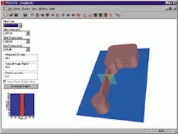
A 2-D simulation provides information on linewidth, sidewall angles, and presence of standing-wave effects. A 3-D simulation can model the patterning of features off-limits to 2-D modeling, such as contacts, 90° bends, and other more-complex shapes (see Fig. 1). A 3-D model also has application to finite lines. "There are some important lithography problems, such as corner rounding and line-end shortening, that can only be solved in a 3-D simulator," says Mack.
Lens aberrations are entered into Prolith as a pupil function and can take one of two forms: a 36-term Zernike polynomial or an output file from Code V optical-design software (Optical Research Associates; Pasadena, CA). The ability to model wavefront aberrations is as important to designers of lithographic lenses as it is to process engineers; only lithography-simulation software can directly relate lens-design criteria to lithographic performance. Other relevant lens properties include partial coherence and the distribution of illumination light in the lens pupil (variations of which include off-axis, annular, and quadrupole).
Resist properties included in the Prolith model fall into three categories, according to Mack. First are the optical and kinetic properties of the resist, which include refractive index, absorption, and exposure rate, as well as how the optical properties change upon exposure (for example, bleaching of resist). Second are thermal properties; third are development properties that relate to resist tone (positive or negative) and contrast.
Properties of the substrate on which the resist is coated also come into play for modeling. The resist sits on top of a stack of various thin layers such as polycrystalline silicon (poly-Si) or oxide, all on a base of silicon (Si). "The complex refractive index as a function of wavelength and the thickness of each layer must be known," explains Mack. Prolith can perform either scalar or vector operations of reflections throughout the film stack, with the choice left up to the user.
The characteristics of the chosen lithography tool affect the final image, too. While a wafer stepper holds the photomask and wafer still during exposure, a scanner moves them in synchronization, allowing a larger field to be exposed and some aberrations to be averaged. Wafer vibrations affect imaging, as do shifts away from the plane of best focus. All these effects are included in the software model, says Mack. In addition, the software can simulate the effects of phase-shifting photomasks and multiple exposures made while changing focus in small increments, both of which can improve lithographic image quality.
The software is being used to model optical lithography at 157 nm and in the extreme ultraviolet (13 nm) and has found use outside the IC industry in such applications as holographic recording and the making of microelectromechanical systems. Its simulations are tested against experiment on a regular basis. "Most of the validation work is carried out by our customers," says Mack, adding that many users of the software publish technical papers that include Prolith results.
Lasers and links
Much further along in the chipmaking process, at the point when all lithographic patterning has been finished, the IC manufacturer must face the problem of chip defects. Specks of dust, resist flaws, or other imperfections in the lithographic patterning can cause particular chip elements to be inoperable. For some chips, this is not an uncommon outcome. For example, a dynamic random-access memory (DRAM) chip having many millions of memory elements may wind up having more than one nonfunctioning element.
Makers of DRAMs have sidestepped this problem by designing extra rows, columns, or blocks of memory elements into their chips. They also include a decoder circuit on the chip containing links that can be severed to reprogram the circuit. This reprogramming not only deactivates the nonfunctioning memory elements, but also activates additional functional memory elements, thus repairing the chip. The links are typically severed using pulses of focused near-infrared light emitted by solid-state lasers.
Historically, such links were made of poly-Si and were severed by Nd:YAG lasers emitting at 1.064 µm. Software models developed to model the interaction of laser light with poly-Si produced results that at least partially matched with reality. But memory chips grew in size, and the techniques used to manufacture DRAMs of 64-Mbit capacity and larger required a change in link material from poly-Si to metal, a material not well-suited for processing with 1.064-µm light. The existing software models could give no guidance on how to improve the process, according to Ed Swenson, vice president of research and development at Electro Scientific Industries Inc. (ESI; Portland, OR), a maker of laser-based link-processing equipment. As a result, ESI scientists had to develop their own model.
The structure around a link consists of an upper transparent dielectric layer, the link itself, a lower transparent dielectric layer, and the Si substrate. The dielectrics can be single- or multilayer. The link is typically 0.8-2 µm wide and 0.5-1.5 µm thick, with a pitch dimension of 2.5-5 µm. The focused laser spot must be sized to sever a single link without damaging those on either side. Below a certain threshold energy, the laser pulse will not cut the link; above another higher threshold energy, the pulse will not only sever the link, but will also cause damage to the Si substrate, as well as other adverse effects. One result of a good software model is the accurate determination of these two thresholds and thus the safe operating window.
The model developed at ESI aids its users in three ways. First, it calculates the optimum thickness of the dielectric layers. Due to optical interference, the portion of light absorbed by the link in certain link structures can vary by a factor of two as a function of upper dielectric thickness and by more than a factor of four as a function of lower dielectric thickness; the intent of the optimization is to maximize the portion of light absorbed by the link and minimize the portion absorbed by the Si substrate. Second, the model provides thermal and stress analysis of the link and surroundings as it is severed by the laser pulse. Finally, it offers a way to optimize laser parameters.
Wavelength effects come to the fore
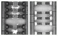
Optimizing laser parameters became very important to ESI, according to Yunlong Sun, senior scientist and the developer of the new software model. When laser wavelength was varied, the model predicted that the use of wavelengths near 1.3 µm could raise the silicon damage threshold by a factor of two and higher, depending on the details of structure (which include dopant levels in the Si substrate). The cause of this increase was shown to be the much-higher optical transmission of Si at wavelengths longer than 1.2 µm, a result of the material's bandgap structure. The model also predicted that switching to 1.3-µm light would have little effect on the processing of the link itself, as the light absorption of most metals does not vary much in the 1-2-µm range.Testing bore this out, and, as a result, ESI now builds longer-wavelength lasers into its link-processing systems and holds patents on the technology. These lasers include Nd:YLF (yttrium lithium fluoride) emitting at 1.321 µm and Nd:YVO4 (vanadate) emitting at 1.343 µm, which are incorporated into link processing systems that can sever up to 7500 links/s (see Fig. 2).
Swenson notes that the accuracy of the software model is checked by comparing its calculations to results collected from dozens of customer sites. He adds that ESI is extending the same software modeling technique to predict the effects of third- and fourth-harmonic ultraviolet (UV) Nd:YAG lasers as they drill vias (holes for IC interconnects on circuit boards) in resin-coated copper foil and other materials. The company has developed equipment that can drill 40-µm vias in 70-µm foil with a roundness better than 90% and believes that its modeling capability will help to further improve the UV laser-via-drilling process.
About the Author
John Wallace
Senior Technical Editor (1998-2022)
John Wallace was with Laser Focus World for nearly 25 years, retiring in late June 2022. He obtained a bachelor's degree in mechanical engineering and physics at Rutgers University and a master's in optical engineering at the University of Rochester. Before becoming an editor, John worked as an engineer at RCA, Exxon, Eastman Kodak, and GCA Corporation.

