Optics software models photovoltaic light trapping
BHUSHAN SOPORI
Light trapping is essential to the performance of photovoltaic (PV) devices, and it presents a set of problems that cannot be adequately addressed by conventional optical design software. Cells and modules used for converting solar energy into electricity generally include intentionally rough or textured surfaces to enhance light trapping. Light trapping can also occur in semiconductor processing such as in rapid thermal processing if the wafer is not polished on both sides. But the rough surfaces also make optical analysis far more complex. Researchers at the National Renewable Energy Laboratory (NREL; Golden, CO) have developed a computer program that specifically addresses light trapping in solar cells and which they hope to expand further for analysis of RTP furnaces.
To increase light trapping, nearly all solar-cell designs now also include antireflection coatings and reflective back surfaces. Generally available optical modeling software does not work for cells with layers less than about 3 µm thick nor for cells with metal reflective backing, two important features of many new photovoltaic cell designs.
Most tools for optical analysis are based on simple ray tracing that adequately models reflection and refraction, but this is sufficient for devices with only thick layers. For very thin layers of material, such as antireflective coatings and thin-film semiconductor materials, it is also necessary to consider polarization and interference effects.
Combining ray and wave optics
Wave optics, based on electromagnetic field physics, does adequately account for polarization and interference/diffraction effects in an absorbing medium. Re searchers from radar and other fields have developed algorithms for wave theory, but that approach has generally been considered impractical as a routine analysis tool because it requires enormous amounts of computer time. By essentially solving Maxwell’s equations for nonplanar interfaces, NREL researchers developed a program that effectively applied wave theory to light trapping. This program, however, still made tremendous demands of the computer.
The NREL team developed approximations for practical and effective application of wave optics. The resulting program, PV Optics, is a workable software program that includes wave optics for thin layers to account for interference effects and relies on simpler ray optics whenever they are sufficient.
The other major challenge overcome by PV Optics is adequate analysis of the optics of metal reflective backings. Because the optics of metal layers were not well understood, previous models simply assumed that metal layers were fully reflective. This assumption was based on metallic reflectors being highly reflective in air. NREL researchers showed, however, that at interfaces with high-refractive-index materials such as silicon, metals are not fully reflective. Furthermore, they determined that losses to metal absorption can be multiplied by light trapping because of multiple reflections. So the assumption that all light was reflected and none was absorbed introduced considerable error. As a result, solar-cell developers were frequently surprised to find that their reflective-backing cells were less efficient than expected, sometimes even less efficient than without the metal backing.
Our research, however, showed that assumptions could be made that would be valid for calculating losses in solar cells. By applying either ray or wave physics as appropriate to the thickness of the metal layer, the research team was able to accurately model the optics of a metal layer. By incorporating this assumption into its algorithm, PV Optics effectively analyzes the impact of a metal backing.
PV Optics also determines how each wavelength is being absorbed spatially in the cell and plots light absorption as a function of depth. This information helps to optimize absorption near the (top) collection zone of the semiconductor material to maximize carrier collection by the cell or each of its component layers—a basic part of maximizing electrical generation.
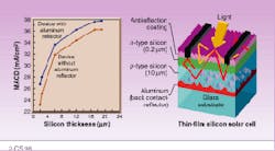
To use PV Optics, a solar-cell designer needs simply to select appropriate cell components being used, indicate whether the surface is smooth or textured, enter the height of the texture, and enter the thickness, index of refraction, and absorption coefficient of each of the layers. The program selectively applies ray or wave physics, as appropriate, and calculates the maximum achievable current density for the cell configuration (see figure). The program also plots the reflection, transmission, total absorption, absorption in silicon or other semiconductor, and absorption in metal of the cell as a function of the wavelength of the incident light.
For multijunction devices, the program also plots absorbance by each junction plus total absorbance. An additional plot shows the absorbance by wavelength weighted to typical sunlight—the key data for calculating solar-cell efficiency for various semiconductor materials. Finally, the program shows photon absorption as a function of depth within the semiconductor layer—the key parameter for determining the ideal thickness of the layer. For thin-film devices with total semiconductor layer thickness less than the light coherence length, the software switches to an alternate program based totally on wave theory. All of these data can then be exported to other programs for analysis of the cell’s or module’s electrical response to the absorbed sunlight. PV Optics runs on a PC with Windows and requires 8 Mbyte of RAM.
Practical applications
PV Optics is immediately usable by any photovoltaic researcher or solar cell or module manufacturer working with crystalline, multicrystalline, or amorphous silicon, including multijunction designs (this includes nearly all devices currently produced commercially). The software will quickly and accurately analyze light trapping for current or prospective designs, and the model will provide all the key data to maximize efficiency of the design.
Program output is directly usable in electronic modeling software such as AMPS (Analysis of Microelectronic and Photonic Structures), which was developed by Pennsylvania State University for the Electric Power Research Institute (Palo Alto, CA) to calculate actual electrical generation. Thus a cell designer can directly predict module performance from measurements made in air prior to module construction. The software is also directly applicable to design of optical detectors and certain types of display devices.
The PV Optics model is already set up to handle multilayer thin-film materials such as cadmium telluride and multijunction compound materials such as gallium indium arsenide/gallium phosphide, whether their interfaces are textured or planar. These capabilities will be added to standard future versions of the software after verification of values but are available now upon request if a user needs to analyze a particular compound semiconductor material.
Rapid-thermal-processing (RTP) furnaces use light energy to directly heat an individual object rather than heating all the space around the object as a conventional oven would. They are widely used by the microelectronics industry for device processing and fabrication, and they are gaining popularity with the solar-cell industry as well. Because PV Optics model analyzes the light and, therefore, heat trapping of the incoming light energy, it allows selection of optimal intensity and direction of light for particular processing or fabrication steps. Adding this capability to a future version of the software should allow significant improvement in the efficiency of RTP. NREL’s own optical processing furnace, which takes RTP a step further by taking advantage of direct effects of light energy to enable lower temperature and new reactions, will benefit even more.
PV Optics could easily be adapted to model textured lenses such as the Fresnel lenses used in solar concentrator systems. In other applications, the model could also be used by jewel cutters to determine an ideal cut or investigate new designs without having to sacrifice valuable gems.