PHOTONICS APPLIED: MICROELECTRONICS PROCESSING: Laser direct structuring creates low-cost 3D integrated circuits
DOUG GRIES
The need to create more functionality in tighter spaces is challenging mechanical and electronics designers to find innovative technologies to assist them. Laser direct structuring (LDS) has been around for 10 years but has only recently seen an increase in the diversity of its application beyond the fabrication of integrated cell phone antennas, which constitutes the largest application for this emerging technology.
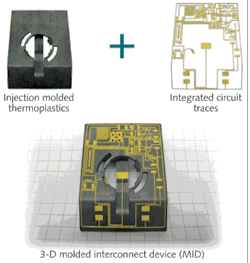
In LDS, a three-dimensional molded interconnect device (3D-MID) is created by taking a plastic injection-molded component and integrating a circuit trace on the surface along the contour of the component (see Fig. 1). This circuit trace is fashioned through the use of an LPKF (Hannover, Germany) laser system to ablate the pattern and apply subsequent metallization that selectively plates only where the laser has traced. In addition, using a high-heat thermoplastic allows for surface-mount components to be added using standard reflow solder. The design and manufacturing advantages are obvious: parts consolidation, miniaturization, weight reduction, reduced assembly time, increased reliability, and the potential for overall system cost reduction for emerging applications in the medical, automotive, industrial, and military/defense markets.
Direct structuring in 3D
The LDS process begins with a component that has been injection-molded with a specialty thermoplastic compound. This thermoplastic has an organometallic additive compounded into it throughout the polymer matrix. The additive is essentially a metallic particulate encapsulated with an organic coating and does not significantly alter the inherent properties of the thermoplastic. A broad array of polymer families are available, including liquid-crystal polymer (LCP), high-heat nylon (PA6/6T), polyphthalamide(PPA), polybutylene terephthalate (PBT), PBT/PET, and polycarbonate/ABS plastic.
The part is then fixtured in an LPKF laser system in preparation for surface activation (LPKF owns the patents for use of a laser to make circuit patterns on molded components). Prior to surface activation, the laser is programmed to write the pattern based on CAD data supplied by the designer. This process is called "hatching" and is a key to producing well-structured parts because there is an optimal pattern for the laser to follow depending on the circuit trace layout.
Circuit patterns are fabricated using a 16 W diode-pumped neodymium-doped yttrium orthovanadate (Nd:YVO4) laser. An acousto-optical Q-switch provides pulses with a very high pulse-to-pulse stability (better than 1.5%)–important for uniform activation of the parts. The 1064 nm source has a pulse repetition rate between 20 and 100 kHz, and the system uses a high-speed scanner and optical z-axis for 3D beam delivery. With a maximum scanning speed of 4.0 m/s, a 65 μm beam diameter creates the circuit traces and pad positions in preparation for the next step in the process.
First-pass plating gives a good indication of whether the laser parameters need to be adjusted or optimized for the specific material to be etched. Based on the breadth of LDS injection-molding grades now available, power settings range from 2.0 to 7.0 W and frequencies between 40 and 100 kHz, with speeds between 2.0 and 4.0 m/s. Each material has a specific recommended setup with these three parameters, but that can be adjusted if the optimal etching surface is not achieved with the hatching pattern.
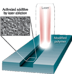
When the laser contacts the surface of the injection-molded component, activation occurs with two distinct effects. First, the energy of the laser breaks the organic coating of the organometallic particulate, exposing the metallic particles on the surface of the part. Second, the part is etched along the laser trace, in effect creating a textured surface topography that is receptive to metallization (see Fig. 2). Based on the type of material and the laser settings (primarily the power settings), either a very small channel is formed (up to 10 μm in depth) or a very small ridge is formed due to ablation effects. Because the organometallic surface is unaffected in nonlasered areas, we now have a part that is primed to selectively plate only where the laser has traced.The first step in the patented SelectConnect metallization process is deposition of an electroless copper layer; the textured surface with metallic particles creates an electronegative potential that initiates the copper deposition. Because copper has relatively poor oxidation resistance, most 3D-MIDs are subsequently plated with electroless nickel. A final immersion gold layer is optional, providing excellent oxidation resistance in addition to ideal landing surfaces for surface-mount components. For these plating layers, typical thickness builds are 100-600 micro-in. of copper, 50-100 micro-in. of nickel, and 3-8 micro-in. of gold. Thicker builds of copper and nickel are possible if an application requires this for various reasons, such as the ability to carry larger currents. Immersion gold build is limited to 8 micro-in. because it is not an autocatalytic process. Electroless gold plating is a viable option if thicker gold builds are required.
Circuit applications and constraints
The most common LDS applications today are for wireless antenna and current-carrying circuits. By taking a functional interior plastic component in a cell phone and applying the antenna pattern directly to it, we now have an integrated antenna that has eliminated the need for a separate metal antenna. The benefits of LDS play right into this application area, where parts consolidation, miniaturization, and reduced assembly operations are critical to volume production and reducing cell phone costs. In addition, LDS technology is easily amenable to rapid prototyping to configure different antenna patterns. Today, the vast majority of LPKF lasers using LDS techniques are in China producing cell phone antennas.
Another functional attribute of LDS–the ability to create current-carrying circuitry monolithically with functional circuitry–is now expanding the application base beyond cell phone components. In essence, LDS combines a mechanical plastic component with an electronic circuit that would, without LDS, require a separate circuit board or flex circuit.
Faced with packaging constraints, designers naturally push the envelope on laying the circuitry and would like increasingly smaller lines (the circuit traces) and spaces (the gap between the traces). Because the LDS beam diameter is 65 μm, this is the theoretical absolute smallest linewidth, but in reality the minimum linewidth is actually at least twice the beam diameter due to the need to make at least two passes of the laser to create an intact circuit. Regarding gaps, the limit is based on creating a circuit pattern that gives enough latitude such that the plating process does not result in bridging two parallel circuits (a short circuit). Based on experience to date, the smallest line and space pattern that is considered suitable for production is 0.008 in. (8 mil) lines and 0.010 in. (10 mil) spaces. It is technically possible to go slightly smaller than this; however, very careful consideration needs to be paid to all aspects of the design to create a process robust enough for high yield during production.
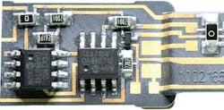
With the added flexibility of adding surface-mount components, we can essentially fashion a circuit board as part of our mechanical plastic component (see Fig. 3). The polymers LCP and PPA can withstand typical reflow solder temperatures and for applications requiring lead-free reflow solder, Ultramid PA6/6T resin from BASF can withstand the necessary elevated temperatures. Vias in the plastic component can also be created to connect both sides of the component. This gives the designer added flexibility in that circuits can now be fashioned on both sides of the part. Because the laser has to activate the surface of the via, the via simply is created with a conical design on one or both sides.Within the automotive realm, we are seeing applications such as steering wheel hubs, brake sensors, and positioning sensors. Industrial applications include integrated connectors, automated pipettes, motion sensors, and RFID antennas. In one automotive application, high-temperature, high-humidity (85ºC/85% relative humidity) testing of a rotation brake sensor showed zero defects in 300 pieces after 1000 hours. The material used was Vectra E840i (LCP). These results show the robustness of this process and have encouraged further automotive developments at SelectConnect.
Five years ago, there were just two unique applications that incorporated LDS technology for integrated circuit design; today, there are 25 and the list continues to grow.
Doug Gries is VP of business development for SelectConnect Technologies, 600 S. Vermont St., Palatine, IL 60067-6950; e-mail: [email protected]; www.selectconnecttech.com.


