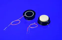
Morgan Technical Ceramics ultrasonic sensors measure gas flow
Ultrasonic sensors perform gas flow measurement in acoustic anemometry systems, SMART metering systems, and air-coupled level measurement of liquids and solids. The 20-mm-diameter sensors provide accurate information in one dimension (a line), two dimensions (an area), or three dimensions (a volume). They use high-performance piezoceramic materials and have no moving parts.
Morgan Technical Ceramics
Fairfield, NJ
[email protected]
-----
Morgan Technical Ceramics unveils new line of ultrasonic sensors for gas flow measurement
Morgan Technical Ceramics (MTC) announces its new line of ultrasonic sensors for gas flow measurement, ideal for integrating into acoustic anemometry systems and SMART metering systems for measuring natural gas usage, as well as air-coupled level measurement of liquids and solids. The transducer transmits and receives ultrasonic waves across a gas channel for time of flight measurement.
The new, 20mm diameter sensors provide accurate information in one dimension (a line), two dimensions (an area), or three dimensions (a volume). Using the latest high performance piezoceramic materials, the new ultrasonic sensors offer exceptional mechanical and electrical properties, excellent bandwidth, and sensitivity for accurate measurement readings. The materialsâ outstanding temperature stability ensures accurate measurement across the whole spectrum of conditions a meter may be exposed to.
With no moving parts, the new ultrasonic sensor is not subject to wear making it more reliable than alternative methods of flow measurement. The sensors suffer no pressure loss, offer nearly maintenance-free operation, and are more accurate than many competing systems. In addition, they are more adaptable to the electronic display of energy favored for SMART meters.
Using innovative tools like 3D finite element analysis, MTCâs transducer research and development team works closely with customers to provide virtual prototype transducers, cutting down development time considerably. Design engineers can adjust the sensorâs architecture, manufacturing process, and material properties for a particular application, and can produce the sensors in low, medium or high volumes.
About Morgan Technical Ceramics
Morgan Technical Ceramics manufactures components and sub-assemblies using an extensive range of materials, including structural and piezoelectric ceramics, dielectrics, braze alloys, and specialist coatings. It works with manufacturersâ design and R&D teams at local, national and international level on projects from concept and feasibility studies through prototype development to full production. The business employs some 2,500 people and has 23 manufacturing sites worldwide across Europe, the US, Mexico, China and Australia.
Morgan Technical Ceramics is a business within the Morgan Ceramics Division of The Morgan Crucible Company plc, one of the world's leading advanced materials companies. The company specialises in the design, manufacture and marketing of ceramic and carbon products which are used in a wide range of applications, from transport and telecommunications to fire protection and medical instruments. Morgan Crucible is listed on the London Stock Exchange in the engineering sector.
-----
Subscribe now to Laser Focus World magazine; it's free!
