Silica-on-silicon remains a staple for making waveguides
Terry Caves
Designing the basic building blocks of components so that the refractive index of the core and cladding are the same helps manufacturers achieve economies of scale.Even in light of the recent upheaval in the telecommunications market, the world of optical networking continues to face a major challengenamely, the increasing demand for optoelectronic components and subsystems for high-bandwidth services and the inability of suppliers to produce at required volumes. These problems can be traced to the scalability limitations of dominant component-manufacturing processes. Thin-film filter processing, for example, is notorious for its dependence upon manual labor and limited production volumes, both of which contribute to high fabrication costs.
Containing costs
One way to contain costs is to combine planar waveguide architecture with automated semiconductor processes. Perhaps the most common material choice involves silica on silicon. Although some component manufacturers instead use silicon on silicon to produce a smaller waveguide, this material combination does not support the writing of Bragg gratings onto the waveguide because space is too limited for the use of photolithography. There also is a higher loss per centimeter of device area.
With the silica-on-silicon process, achieving the appropriate refractive index to form a component waveguide involves the application of layers of silica to a base of a standard 6- or 8-in. silicon wafer through several electrochemical processing techniques. The two most common classes of deposition processes are plasma-enhanced chemical-vapor deposition and flame hydrolysis. The former has the advantage of maturityit has been used in the semiconductor industry for years. Flame hydrolysis, on the other hand, still requires a hodgepodge of equipment. It also can have problems achieving wafer uniformity in thickness and refractive index, both of which are key to waveguide performance.
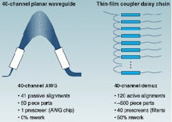
FIGURE 1. Devices such as this integrated planar-waveguide 40-channel AWG have a much smaller footprint than similar devices produced with conventional thin-film processing.
One way to leverage batch processing is to grow the constituent devices that comprise any given component on the same wafer through the same process cycle (see Fig. 1). The key is to design the basic building block of the optical component so that the refractive index of the core and cladding are the same. If one can treat as many as 100 photonic circuits on a wafer, and standard semiconductor equipment allows for the processing of 25 silicon wafers simultaneously, a single process cycle could fabricate tens of thousands of variable optical attenuators (VOAs) simultaneously.
The planar waveguide process also must deal with the integration of optical junctions, which, from a design standpoint, are easier to address during the material processing stage than after the fact. By designing these junctions into the material treatment process, the manufacturing process automatically eliminates the considerable rework that would be necessary to establish these interfaces manually.
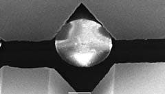
FIGURE 2. Fiber alignment accuracies can be within 0.05 µm using V-grooves that have been etched into the passive component. In comparison, mechanical alignment techniques, such as those used in thin-film processing, have difficulty achieving submicron accuracy.
Using a chemical-physical alignment process, alignment chambers known as V-grooves are etched into the wafer using controlled chemical reactions that create an alignment path to the waveguide (see Fig. 2). The resulting V-groove guides promote passive alignment, in which multiple fibers virtually self-align to the waveguides. This approach supports alignment accuracies within 0.05 µm. In comparison, mechanical alignment techniques, such as those used with thin-film processing, have difficulty achieving submicron accuracy. V-groove connections also are subject to far less signal loss, which enhances their efficiency.
Pros and cons
The flexibility engendered by on-chip connections and batch processing opens a world of possibilities in the integration of passive components.
As an example, a standard 40-channel V-multiplexer is typically produced through the union of discrete arrayed waveguide (AWG) and VOA components. Simply integrating the AWG and VOA circuitry on the same chip eliminates as many as 120 redundant optical interfaces. The footprint of the component is also smaller, yet designers can still address requirements for higher channel counts.
Paradoxically, because Zenastra's planar waveguide silica-on-silicon architecture was developed to address the market demand for higher-channel devices, the company's components are subject to a greater insertion loss in lower-channel devices. As an example, a standard 8-channel AWG component will experience more insertion loss than its thin-film process equivalent5 dB of loss compared to less than 1 dB loss. This is a by-product of the planar architecture, which immediately splits the signal into several independent channels. This insertion loss becomes equal to that of the thin-film component when components approach the 30-channel count. Unlike the planar waveguide architecture, though, thin-film architecture continues to experience cumulative insertion loss as the channel count rises and more discrete components are added to the device.
On devices with large channel spacings, say 200 GHz and above, or channel counts below 16, thin-film processing retains a cost and performance advantage over planar waveguide manufacturing. Narrow the channel spacing to below 100 GHz, and the thin-film approach has difficulty meeting the necessary requirements for adjacent channel isolation and passband flatness.
Planar waveguide components also can be susceptible to birefringent stresses, and hence phase-delay distortion and polarization-dependent loss (PDL). The reason lies with the subtle change to the refractive index that can occur following the wafer-processing stage. This issue is addressable with the addition of an annealing process to heat the wafer to the right temperature to release accumulated stresses. Any temperature-induced PDL, which also could affect the refractive index of the waveguide, is eliminated by the installation of Peltier coolers, which maintain the wafer temperature to within 2°C.
The future
Given current market conditions, perhaps the most compelling advantage to the silica-on-silicon approach to manufacturing and component architecture remains its fabrication speed and flexibility.
Given time-to-market pressure, original equipment manufacturers are increasingly interested in outsourcing component manufacturing rather than expending the resources and energy to develop them in-house.
Furthermore, many are demanding the integration of active devices such as lasers and detectors into controllable modules to facilitate the tasks of network monitoring and control.
By leveraging the advantages of a scalable and automated manufacturing process and a flexible component architecture that allows a reduced component footprint and cost, it becomes possible to deliver low-cost, integrated passive-active components to address the extensive market for systems intelligence at the metro level.
To date, Zenastra has leveraged its planar-waveguide manufacturing process to achieve a variety of passive optical components, as well as at least one integrated passive and active device. The passive products include a 16-channel AWG multiplexer/demultiplexer; a 2 x 2 thermo-optic switch; an 8-channel VOA array; and a 100-GHz single- and 4-channel optical add/drop multiplexer/demultiplexer (OADM). The integrated passive products include a configurable OADM and a VOA multiplexer.
Although integration of passive and active components requires a hybrid fabrication process, the planar waveguide technique can become a fundamental building block. Because alignment wells can be embedded during the passive stage, it becomes easier to position lasers and detectors on the device. Active-component alignment is also more precise.
TERRY CAVES is vice president of engineering and manufacturing at Zenastra Photonics Inc., 2305 St. Laurent Blvd., Ottawa, Ont., Canada K1G 4J8; e-mail: [email protected].


