FLAT-PANEL DISPLAYS: Large-area color nanotube FED debuts
The Samsung Advanced Institute of Technology (SAIT) at the Samsung corporate R&D center (Suwon, Korea) has unveiled a large-area color carbon nanotube field-emission display (CNT-FED). At the International Display Workshop '99 (December 1999; Sendai, Japan), the research institute showcased a 9-in.-diagonal, full-color prototype device with a 200 x 120-µm pixel size and 576 x 240 line resolution (smaller pixels are possible).
The CNT-FED offers three colors at every pixel, and color separation occurs without crosstalk. Other features include a fast response rate, low power consumption, wide viewing angles, a wide operating-temperature range, and display brightness of 200 cd/m2 at 3 v/µm.
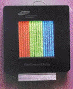
The SAIT had demonstrated a 4.5-in. CNT-FED at two earlier conferences in 1999 (see figure). According to Jong Min Kim, director of the SAIT display laboratory, and colleagues, scalability of the technology is no problem, and an even larger CNT-FED should be demonstrated soon.
Interest in carbon nanotubes is growing because of their unique electrical properties. The benefits range from large aspect ratios to high chemical stability, thermal conductivity, and high mechanical strength.1 Until recently, though, the fabrication method, particularly large-area synthesis, has held back low-cost development of FEDs with vertically aligned CNTs. Samsung seems to have resolved this issue with the displays recently demonstrated.
Device structure
The CNT-based, diode-type flat-panel-display structure developed by the firm has two sets of glass plates, one with single-walled nanotubes on the patterned cathode glass and the other with phosphor-coated indium tin oxide stripes on the anode glass. Spacers keep a 200-µm distance between the patterned phosphor and the carbon-nanotube/patterned-metal plates. The pixels are formed at the intersection of cathode and anode stripes.
Samsung fabricates the fully sealed CNT-FEDs using nitrocellulose paste that contains single-wall CNTs. Where other manufacturers have grown aligned CNTs with chemical-vapor deposition at temperatures higher than 700°C, the company's displays are fully scalable at processing temperatures below 415°C. (Display applications using sodalime glass require processing temperatures below 500°C). vertical alignment of the nanotubes is accomplished by squeezing the paste through a metal mesh, surface rubbing, and/or conditioning by an electric field.
The Samsung CNT-FED fabrication process produces displays with a low turn-on voltage, high brightness, and high stability. Jong Min Kim says there is no degradation of nanotube emission over time at the operating voltage. The operating voltage of the diode FED is 1.5-2.0 v/µm. In triode mode, this bias goes up to several kilovolts.
The 4.5-in. CNT-FED produced a brightness of 1800 cd/m2 at 3.7 v/µm (a current density of 90 µA/cm2) across the entire area of a 4.5-in. panel for the green phosphor/indium tin oxide-coated glass. Current fluctuation was approximately 7% over the cathode area. Brightness reached 900 cd/m2 for the blue phosphor and 800 cd/m2 for the red phosphor under the same conditions.
REFERENCE
- W. B. Choi et al., Appl. Phys. Lett. 75, 3129 (Nov. 15, 1999).
About the Author
Paula Noaker Powell
Senior Editor, Laser Focus World
Paula Noaker Powell was a senior editor for Laser Focus World.
