Organic LEDs:Doped OLEDs overcome limitations of traditional devices
STEPHAN RENTENBERGER
High efficiency and lifetimes of several years are only two prerequisites of current and future applications for organic light-emitting diodes (OLEDs). The use of p‑i-n OLED technology overcomes several issues that previously limited traditional nondoped devices and opens new possibilities for the next display generation that will depend especially upon white-light, top-emitting OLEDs.
The steadily growing market for OLEDs currently focuses on three major fields of application: passive-matrix displays, which already can be found in a variety of portable MP3 player displays and mobile phone subdisplays; active-matrix displays, which are required for larger displays like computer monitors or television screens; and lighting/signage applications, which are expected to enter the mass market within the next few years.
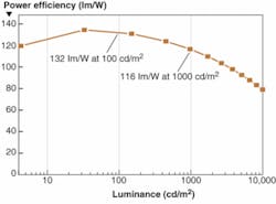
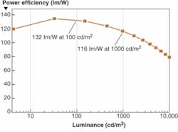
The main challenge for passive-matrix displays is the required luminance of 20,000 to 60,000 cd/m2 and above. This requirement raises the need for very high efficiencies, even in a range where common non-p-i-n OLED stacks show a strong power-efficiency roll-off. Standard, bottom-emitting active-matrix displays, on the other hand, are limited by a reduced aperture ratio because of the relatively large area consumed by the nontransparent thin-film transistors (TFTs) on the backplane. Such displays therefore benefit from top-emitting structures (fabricated on top of the TFTs), which increase the aperture ratio and thus require less pixel brightness, increasing the lifetime of such devices. For illumination, lighting, and signage applications the main target, in addition to power efficiency and lifetime, is good color tunability with a high color-rendering index in the case of white light.
Recently, thermal stability has become a focus of the OLED community, pushed by possible automotive applications. Most of these applications can be combined with flexible substrates and even partially transparent structures, which are just two advantages of OLEDs over their inorganic counterparts. Thus, new applications are opening for flexible displays, as well as curved and bendable lighting/signage devices that will garner increasing interest in the future. Lifetime and price competitiveness are common issues that must be satisfied for all OLED applications.
p-i-n OLED technology
The p-i-n OLED approach allows fabrication of OLEDs that fulfill all these requirements. Through the introduction of doped charge-transport layers, the charge-carrier injection barriers are reduced and the voltage drop over the transport layers is minimized.1 The p‑i‑n approach leads to more freedom in the choice of electrode work functions. The p-i-n structures commonly consist of a p-doped hole-transport layer, an intrinsically conductive emission zone, and an n-doped electron-transport layer. This approach yields a reduction of the operation voltage for fluorescent and phosphorescent devices, nearly down to the physical limit of the photon energy.
Introducing additional interlayers between the transport and the emission layer means charge carriers are confined to a defined emission zone, raising the efficiency without losing the low operation voltage.2, 3 In addition, the devices have lower onset voltage and a much steeper luminance-voltage characteristic compared to nondoped OLEDs.4
For instance, in a green phosphorescent OLED using fac-tris(2-phenypyridine) iridium (Ir(ppy)3) as the emitter, the highly conductive transport layers yield another advantage unique to doped OLED structures-an operating voltage independent of the transport-layer thickness (see Fig. 1). An independent operating voltage allows the use of microcavity effects, which further increase efficiency and either prefer or suppress definable color ranges.
One of the major drawbacks of OLEDs has been limited operational lifetime. Even though the lifetime is defined by a luminance decrease of 50% and not by a total blackout, 20,000 hours (more than two years) of continuous operation at 500 cd/m2 is a common target for handheld consumer devices. For TV screens, at least 50,000 hours is the target. By using newly synthesized materials in combination with optimized structures, lifetimes well over a million hours for red, up to 42,000 hours for green, and up to 40,000 hours for blue OLEDs were achieved at an initial brightness of 500 cd/m2. Lifetimes for white are in the range of 40,000 hours at 1000 cd/m2.
The main drawback of traditional dopants is the tendency to diffuse as temperature increases. This, as well as low glass transition temperatures (Tg) for electron-transport materials, points to the need for new materials to successfully position p-i-n technology in the market. Initial applications of p-i-n OLED technology using cesium-doped electron-transport layers demonstrated drastically reduced lifetimes above 60°C. In addition, acceptor molecules like 2,3,5,6-tetrafluoro-7,7,8,8-tetracyano-quinodimethane (F4-TCNQ), which were used as dopants for the hole-transport side, have an evaporation temperature below 100°C.
Newly synthesized materials, such as the Novaled-developed n-dopant NDN‑1 and p-dopant NDP‑2 exhibit an evaporation temperature well above 100°C, offering compatibility even with automotive requirements. The second bottleneck involves electron-transport materials such as aluminum tris(8-hydroxyquinoline) (Alq3) that exhibit poor electron mobility and are not sufficiently dopable. Next-generation host materials such as NET-9 may meet such requirements, however, because they are dopable and exhibit a Tg of 165°C.5
Top emission
Because active-matrix OLED displays feature numerous bus lines, capacitors, and TFTs, the overall aperture ratio of bottom-emitting active-matrix OLEDs falls in the range of 35% to 40%, and changing to top emission can double the active area. Potential application areas include nontransparent substrates for flexible OLED applications and semitransparent OLED displays. Created by inverting a p-i-n OLED stack, n-i-p structures allow fabrication of OLEDs on an even wider range of substrates such as amorphous silicon (a-Si) for n-channel TFTs.
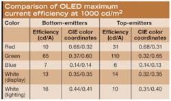
A lot of effort has been put into the development of bottom-emitting devices and the performance of top-emission OLEDs is generally not as good. But driven by the need for active-matrix displays and nontransparent device substrates, top-emitting OLED structures are generating interest. Efficiencies of top-emitting p-i-n devices have begun to compete with bottom-emission geometries (see Fig. 2 and table). They are expected to eventually overtake bottom-geometry devices because of higher outcoupling efficiency resulting from the absence of substrate modes and the use of a highly reflective bottom anode in combination with a transparency-enhanced top cathode. Enabled by the high conductivity of the transport layers used by the p-i-n technology, flexibility in tuning the transport-layer thickness allows further optimization of the light outcoupling. Current lifetime measurements exceed 100,000 hours for red and green (at 500 cd/m2), 16,000 hours for blue (at 500 cd/m2), and 18,000 hours for white (at 1000 cd/m2).
null
null
White emission
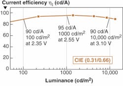
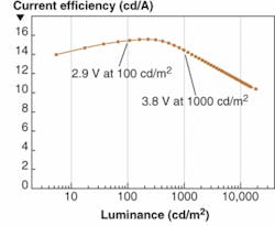
White OLEDs are growing in importance, especially for emerging lighting applications, and two major approaches are under development. There is need for highly efficient white OLEDs that can be used in a liquid-crystal-display backlight. By combining three emitting materials, namely a fluorescent blue, a phosphorescent green, and a phosphorescent red-emitter-matching the absorption maxima of the three color filters-a color rendering index (CRI) of 95 has been achieved with International Commission on Illumination (CIE) color coordinates of 0.35/0.37. By combining top and white emission from a two-color fluorescent white OLED, efficiencies of 14 cd/A at 1000 cd/m2 were reached (see Fig. 3).
On the other hand, OLEDs can act as lighting replacements for conventional sources such as incandescent and neon lamps. In these cases, warm colors around the illuminant A (CIE cc: 0.448/0.407) are required at moderate brightness. With p-i-n OLED technology, it is possible to tune the emission color across a broad range without sacrificing low driving voltages and high efficiencies. For a color coordinate of (0.44/0.41), current efficiencies up to 16 cd/A (at 1000 cd/m2) have been achieved. Because OLEDs emit light from customizable shapes-unlike point-light sources such as incandescent lamps-totally new applications emerge. In combination with curved and bendable substrates, OLEDs are seen as the light source of the future.
The use of p-i-n technology for the fabrication of OLEDs reduces several limitations of nondoped OLED technology. While lifetime and temperature stability have been difficult issues for a long time, the use of new materials enables much improved efficiencies and lifetimes. Especially in the field of top-emitting and white-OLED structures, the high conductivity of the doped transport layers exceeds previous efficiency limits with a higher flexibility in stack optimization and allows the use of a greater variety of substrates.
ACKNOWLEDGMENTS
For their financial support, the author thanks the Freistaat Sachsen, the European Union (framework FP 6), as well as the German Secretary of Education and Research (BMBF).
REFERENCES
1. M. Pfeiffer et al., Organic Electronics 4, 89 (2003).
2. P. Wellmann, et al., J.of the SID 13(5) 393 (2005).
3. J. Birnstock et al., SID 2005 Digest, 40 (4.4L)
4. J. Blochwitz, M. Pfeiffer, T. Fritz, K. Leo, Appl. Phys. Lett. 73(6) 729 (1998).
5. J. Birnstock et al., SID 2006 Digest, 1866 (64.4).
STEPHAN RENTENBERGER is a customer project manager at Novaled, Tatzberg 49, 01307 Dresden, Germany; e-mail: [email protected]; www.novaled.com.
