INTERFEROMETRY: Multipurpose optical tool characterizes MEMS

Uses of microelectromechanical-system (MEMS) devices range from the everyday (crash-sensing accelerometers for automotive airbags) to the specialized (microgyroscopes for military use). As MEMS devices become more complex and precise, so must the tools to test them. Traditionally, these tools take the form of single-purpose, optical-table-size setups. But researchers at Worcester Polytechnic Institute (WPI; Worcester, MA) have developed and refined a multipurpose stand-alone tool that can measure MEMS shape via several interferometric methods and perform optically based vibration and deformation testing as well.
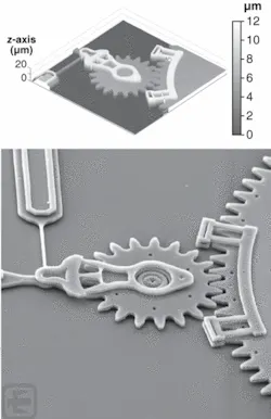
Called a modular interferometric measurement system (MIMS), the tool is capable of phase-stepped Michelson, Mirau, and scanning-white-light measurements of surface shape (with the swapping of interferometric modules). Each configuration has its own merits: Michelson with a large field of view and high precision; Mirau with a high magnification and precision, and easy alignment; and scanning white light (which is based on either of the first two methods) with the ability to measure discontinuous steps (see figure). The vibrometer is also interferometric, and monitors the velocity at a single spot. Minus its operator interface and instrumentation rack, the MIMS, which is based on a vibration-isolated granite chassis, has a footprint of less than a meter on a side.
Environmental testing
The tool has an axial (height) resolution of better than 1 nm, can measure steps of up to 50 µm in size, and has a lateral viewing area of from 20 × 20 µm to 20 × 20 mm, depending on the type of interferometric measurement used. A small environmental chamber holds the MEMS device under test and can subject it to temperatures ranging from -30°C to +120°C, vibrational loading from 1 kHz to 1 MHz, and a vacuum (down to 3 µbar) or dry-gas environment.
A light-emitting-diode source produces a short coherence length of 10 to 20 µm; a halogen lamp provides an even shorter coherence length for scanning-white-light interferometry. “As MEMS are typically composed of several distinct layers and phase-stepped interferometry is limited to measuring one continuous surface at a time, we want a light source that produces interference on the layer being investigated, but not on surrounding layers,” says Adam Klempner, one of the researchers. “This greatly simplifies analyzing the interferometric data when compared to interferograms recorded using a laser as the light source.” For vibration testing, piezoelectric actuators drive the device under test, characterizing their resonant modes.
“We have been studying the effects of thin metal coatings on the dynamic operation of MEMS,” says Klempner. “Typically fabricated out of silicon, MEMS are not good electrical conductors, so metal coatings are commonly applied to surfaces to allow for signal transmission. These coatings, however, often adversely affect the performance of the device, especially devices that require a high Q factor. We are going to publish results on this study in the near future, but I can say that coatings as thin as 5 nm on these beams will significantly reduce the Q factor in vacuum environments. We also do a significant amount of work with outside organizations that are developing high-performance MEMS. We regularly help them with nearly all aspects of the MEMS development cycle, from concept and prototype testing to production device characterization. Recently we have undertaken several long-term studies of MEMS reliability that are showing very interesting results on the effects of aging (relaxation) and thermal cycling of MEMS.”
Future plans include more-user-friendly software, a vacuum chamber capable of reaching down to 1 µtorr (1 torr is approximately 0.0013 bar), and the development of a Fizeau interferometer module to characterize entire 4 in. wafers.
About the Author
John Wallace
Senior Technical Editor (1998-2022)
John Wallace was with Laser Focus World for nearly 25 years, retiring in late June 2022. He obtained a bachelor's degree in mechanical engineering and physics at Rutgers University and a master's in optical engineering at the University of Rochester. Before becoming an editor, John worked as an engineer at RCA, Exxon, Eastman Kodak, and GCA Corporation.
