SHORTWAVE SEMICONDUCTOR LASERS: Improved epitaxy and crystal quality forges the greenest laser diodes
CHRISTIAN WETZEL and THEERADETCH DETCHPROHM
With 405 nm near-ultraviolet gallium nitride/gallium indium nitride/aluminum gallium-nitride (GaN/GaInN/AlGaN) laser diodes in wide use in BlueRay DVD format, and longer blue-wavelength laser diodes gradually appearing, bridging the gap between the blue and red wavelengths remains a lingering challenge.
Bridging the ‘green gap’
Spectrally green emission is readily achieved by increasing the InN fraction in the GaInN alloy of the quantum wells, yet epitaxial growth is tricky there and the alloy easily separates out into nonuniform phases and clusters around the slightest structural defect. Some of the leading teams have seen a benefit in such indium-rich regions, evoking the potential benefits of quantum dots. Our experience at RPI, however, is an entirely different one. We have always seen benefits in thriving for utmost alloy homogeneity and quantum-well perfection. The avoidance of decorating threading dislocations with V-defects has proved key by reducing the number of threading dislocations altogether.
A big help comes from bulk GaN templates grown in hydride vapor-phase epitaxy in which dislocation densities can be as low as 5 × 106 cm-2. We have learned to replicate the good crystalline quality in metal-organic vapor-phase epitaxy of the n side of the laser-diode structure. It is the quantum-well region where, depending on the InN fraction, new dislocations are being generated for wavelengths beyond 515 nm.
For laser diodes, however, and their required high excitation densities, another problem emerges: emission wavelengths are a strong function of the drive current. A deep green or 580 nm yellow LED turns into a 490 nm blue one when the carrier injection reaches some 100 kW/cm2 (optical) or higher as needed for stimulated emission. Early on we recognized that this effect is due to the piezoelectric properties of the c-axis-grown wurtzite material. The discontinuity of the GaInN/GaN quantum wells induces net electric fields across the wells that cannot be screened with any reasonable volume dopant concentration. Its product with the well width results in a piezoelectric dipole that is equivalent to the bandgap offset barrier-to-barrier across the quantum well. The dipole obviously grows with the well width and the piezo field, which in turn grows with the biaxial strain of the well and the InN fraction in the alloy.
In earlier spectroscopy work, we found that this dipole quantity very well describes the up to 300 meV discrepancy of the luminescence emission wavelength and the optical absorption bandgap. In our interpretation, similar to the exciton binding energy of electron and hole, the piezo-dipole induces a Stokes shift of the emission. That is, the current-dependent wavelength shift is a response to an increasing transient-carrier density. A more common description is that of the quantum-confined Stark effect. This instability of the emission wavelength, however, is widely considered a hindrance in lowering the lasing threshold to levels suitable for CW laser diodes.
Optimizing epitaxial growth
To bypass the challenge of the piezoelectric dipole, we developed epitaxy of laser-diode structures along nonpolar axes of GaN such as [11-20] a-axis and [10-10] m-axis, which are perpendicular to the [0001] c-axis. Interestingly, there is a direction somewhere in between where polarization should also have a minimum. The corresponding (11-22) plane has been termed a “semipolar” plane. Bulk GaN templates for all those orientations are readily provided by Kyma Technologies (Raleigh, NC) by slicing thick c-axis-grown boules of GaN or by lateral epitaxial overgrowth as provided by Inlustra Technologies (Santa Barbara, CA).
Our group has learned to grow quantum-well, LED, and laser-diode structures on all those nonpolar growth directions, readily benefiting from even lower densities of threading dislocations.7, 8 Due to their original treading direction along the c-axis of the bulk GaN growth, rotating the crystal after slicing and growth on the side planes starts out with a fresh slate devoid of any treading defects. Even dissected c-axis dislocations are readily buried and remaining dislocation lines are below 105 cm-1.
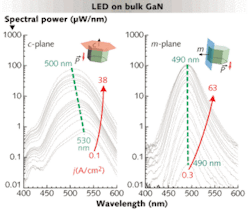
In nonpolar growth, however, new challenges arise. In absence of the piezoelectric dipole, the huge Stokes shift cannot push the emission wavelength across the blue and into the green. It is necessary to compensate for that by either higher InN alloy fractions and/or wider quantum wells, both of which are likely to induce growth instabilities in the GaInN alloy and resulting inhomogenieties. But by properly tuned growth conditions, electroluminescence is observed at 564 nm in a-plane LEDs, 515 nm in m-plane LEDs, and 490 nm in (11-22) semipolar LEDs. Unlike all c-plane structures, the emission wavelength remains stable without variation up to the highest electrical (63 A/cm2) and optical (1 MW/cm2) excitation that we have applied (see Fig. 1). We consider this an ideal precondition for the proper tuning of the laser cavity. Due to the anisotropy of the electronic band structure in the uniaxial crystal, wave propagation differs in all those directions.
Optical dielectric waveguiding within the growth planes can be achieved by thick AlGaN cladding layers contrasting to the GaInN/GaN quantum wells. The risk of layer cracking and consequentially misguided modes is high within such structures. The problems can be avoided by the use of thicker GaInN layers providing enough contrast when cladded by simple GaN alone. Wider wells in polar c-plane structures lead to an undesired reduction of the transition matrix element when charges separate within the piezo field. The result is that carriers recombine nonradiatively by interaction with any defects, or they accumulate to partially screen the piezo field. Those extra carriers, however, pose the additional risk of undesired carrier-carrier interaction such as nonradiative Auger recombination, possibly enhanced by a resonant transition to higher conduction bands.
Here, the nonpolar structures offer yet another advantage: electrons and holes remain mostly centered within their wells, maintaining a high transition rate even in wider wells without accumulation of any transient carriers. In principle, the nonpolar is the ideal solution of the long proposed and tried piezoelectrically matched quantum-well structure.Stimulated emission under optical excitation is the next critical precursor to laser-diode operation. In polar c-plane structures we now achieve stimulated emission at wavelengths as long as 489 nm and in (11-22) plane structures as long as 490 nm. Values for optical excitation densities for lasing thresholds vary strongly with the structure used and associated absorption above the active region. Using 0.1 mJ 10 ns pulses of a 337 nm nitrogen laser, that also excites the GaN layers, we determine external excitation threshold densities in the range of 40 to 1000 kW/cm2. Most notably, in the respective best structures, the threshold does increase only marginally as the wavelength is extended from 400 to 490 nm. This gives high hopes that with the right structure, lasing operation above 500 nm should be well within reach under the proposed approaches.
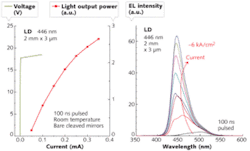
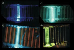
For electrical confinement, we have pursued several approaches, including conventional etched-ridge injection and planar inner-stripe injection. In full laser-diode structures we now reach electrical injection levels of 15 kA/cm2 in pulsed current operation. Bulk GaN substrate again proves ideal for the cleaving of the mirrors, and sapphire-based 446 nm structures can be fabricated (see Fig. 2). This method also enables structures with various emission wavelengths from the violet to the deep green (see Fig. 3).In the meantime, Rohm Co. (Kyoto, Japan) has nearly reached a goal of 500 nm in m-axis growth on Mitsubishi Chemical (Snellville, GA) bulk GaN templates, Osram Opto Semiconductors (Regensburg, Germany) demonstrated a 515 nm direct-emitting green laser diode (see www.laserfocusworld.com/articles/367794), and Sumitomo (Kyushu, Japan) achieved 531 nm in (20-21) plane growth (see www.laserfocusworld.com/articles/368535).9, 10 Defying the challenges of piezoelectric polarization, Nichia Chemical (Tokyo, Japan) recently presented a 510 to 515 nm green laser diode in c-axis growth.11 Most interestingly, the key stated argument that led to this success is the improvement of GaInN crystal quality, an intriguing turn toward our mantra all along.
REFERENCES
- R. D. Dupuis, IEEE LEOS Newsletter, www.ieee.org/organizations/pubs/newsletters/leos/feb03/diode.html (February, 2003).
- M. A. Haase et al., Appl. Phys. Lett. 59(11) p. 1272 (1991).
- S. Taniguchi et al., Electronics Lett. 32, p. 552 (1996).
- H. Amano, M. Kito, K. Hiramatsu, and I. Akasaki, Japanese J. Appl. Physics 28, p. L2112 (1989).
- I. Akasaki et al., Japanese J. Appl. Physics 34, p. L1517 (1995).
- S. Nakamura et al., Appl. Phys. Lett. 69, p. 4056 (1996).
- C. Wetzel et al., J. Crystal Growth 311, p. 2942 (2009).
- T. Detchprohm et al., J. Crystal Growth 311, p. 2937 (2009).
- K. Okamoto et al., Appl. Phys. Lett. 94, p. 071105 (2009).
- Y. Enya et al., Appl. Phys. Exp. 2, p. 082101 (2009).
- T. Miyoshi et al., Appl. Phys. Exp. 2, p. 062201 (2009).
Christian Wetzel is associate professor and Theeradetch Detchprohm is research associate professor in the Department of Physics at Rensselaer Polytechnic Institute, 110 Eighth St., Troy, New York, 12180; e-mail: [email protected]; www.rpi.edu.


