Complex needs drive optoelectronic integration
MARIO DAGENAIS, SIMARJEET SINGH SAINI, ZHENCAN FRANK FAN, FRED SEIFERTH, and SCOTT MERRITT
Wavelength-division multiplexing (WDM) is a technology that allows large quantities of information to be moved from point to point. Forty-channel-WDM systems currently are being deployed, with 80- and 96-channel systems expected to follow shortly. Meanwhile, delivery of broadband services--including voice, data, and video--by optical fiber to every home is another exciting possibility, with deployment imminent. The consequent increase in the sales volume of the optoelectronic (O-E) components involved, together with the increasing complexity of such systems as the number of channels grows, is driving the need for a packaging technology that can provide large-scale, low-cost assembly of O-E components and modules.
One approach to driving down the cost of O-E modules, in which there has been considerable interest recently, is the use of passive alignment techniques. Such techniques are based on components with a large optical mode and do not rely on turning on the laser for accurate coupling to single-mode fibers or waveguides. Instead, the alignment tolerance of large-mode devices allows passive accurate positioning of the device.1
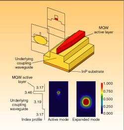
At the University of Maryland, we have developed two alignment-tolerant lasers that require a single epitaxial growth and conventional fabrication techniques.2 The first of these is based on adiabatic-mode transformation from the tightly confined active waveguide to a large, loosely confined underlying waveguide (see Fig. 1). As the waveguide width is reduced gradually by decreasing the ridge width, the power from the active region is transferred adiabatically to the underlying passive waveguide. The active region was optimized for maximum optical gain at a wavelength of 1.55 µm. The dimensions and refractive index of the underlying waveguide were optimized for minimum total loss (mode transformation loss plus coupling loss with a cleaved single-mode fiber).
The fabricated devices showed coupling losses of 3.7 dB to a standard single-mode fiber at 1.55 µm, with the round-trip mode transformation loss of 1.3 dB. The 1-dB alignment tolerance in the transverse direction was calculated to be around 2 µm. For adiabatic transformation between the two waveguides, the taper must be gradual so that radiation losses are low. This means that the mode transformation region is typically large (about 500 µm). For high-speed applications where the device cavity needs to be small, this may be a hindrance.
We have also developed a technique in which the resonant coupling between "supermodes" of a structure transformed the mode over a very short length. For two waveguides of different dimensions, the refractive indices can be adjusted such that their propagation constants are equal. When these waveguides are brought close together vertically so that there is evanescent coupling between the modes of the waveguides, oscillatory power transfer occurs. By keeping one waveguide as the tightly confined active region and the other as the loosely confined coupling waveguide, and by using a specially tapered structure, an efficient mode transformation was achieved over very short lengths with large fabrication tolerances. We de signed a device based on this novel idea with a mode transformation length of 200 µm and mode transformation losses of less than 0.8 dB. These devices had a coupling loss of 3.8 dB to a standard single-mode fiber at 1.55 µm.3
These schemes also make integration of other active and passive devices possible in a single epitaxial growth. The passive devices can be made in the underlying waveguide and the mode can be pushed up or down as required.
Alignment
With optoelectronic circuits becoming increasingly complex, the use of Si waferboard is becoming popular as a platform technology for hybrid integration. Silicon exhibits both good thermal and mechanical properties for this application. Very precise V-grooves for fiber-device alignment can be etched on the surface, and electrical interconnections can be made with flip-chip mounting. Critical positioning requirements are relaxed somewhat by the use of alignment-tolerant mode-expanded structures.
Self-alignment relief patterning is essential for efficient passive assembly, and different research groups are using various types of self-alignment approaches. At British Telecom (Ipswich, UK) researchers have used alignment up stands at an angle to the fiber grooves for packaging an amplifier. The angled alignment upstands allow for the angled facets of the amplifier.4 The V-grooves on either side of the amplifier must be offset. An L-shaped cleave channel was opened on all four corners of the device for accurate control of both the width and the length. The result was a fiber-to-fiber gain of more than 25 dB.
At NEC (Kawasaki, Japan) re searchers have used gold/tin (AuSn) bumps to accurately control the vertical positioning of the optoelectronic integrated circuit (OEIC) chip, which is critical in many applications.5 An AuSn alloy ribbon is punched on the submount and then heated to its melting point, creating solder bumps. Bumps with height accuracy of ۬ µm were successfully fabricated. Another approach, developed at NTT Optoelectronics Laboratory (Ibaraki, Japan), is using a silica-based waveguide on a terraced Si substrate and doing the alignment with alignment features on both the O-E devices and the Si substrate.6
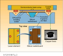
We have developed a method for rapid bonding of semiconductor laser arrays passively aligned to single-mode optical fibers positioned in V-grooves in silicon.7 Our method uses octagonal electrodeposited copper cylinders (bosses) to physically register with precisely etched inverted pyramidal receptacles in the silicon. The microstops and pedestals or standoffs on the silicon waferboard are replaced by rigid copper bosses on the die, while the solder bump reflow is replaced by diffusional bonding to achieve low specific thermal impedance (see Fig. 2).8 The formation of the boss is an additive process that does not require etching side trenches or notches into the die. This also allows an arbitrary choice of orientation of the array to the silicon waferboard crystal axis, eliminating the need for high-precision initial component placement with "vision servoing" or infrared imaging.Fiber Bragg grating
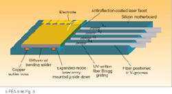
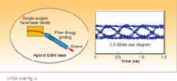
An interesting application of alignment-tolerant structures and silicon waferboard integration is to integrate fiber Bragg gratings with Fabry-Perot semiconductor lasers to make a hybrid distributed Bragg reflector (DBR) WDM laser array (see Fig. 3). We recently demonstrated the operation of such a laser with very good performance.9,10 This laser is comprised of a single-angled facet (SAF) laser diode and a fiber grating with a conical lens. The SAF design provides a very low facet reflectivity (less than 10-4). The laser threshold is about 25 mA, and the laser operates in a stable single longitudinal mode up to more than 100 mA. Side-mode suppression ratio of 50 dB has been achieved.We have also demonstrated high-speed modulation of this laser at 2.5 Gbit/s (see Fig. 4). Using a self-homodyne method, the laser linewidth is measured to be less than 150 kHz, and the dynamic chirp is about 20 MHz/mA—at least an order of magnitude less than standard distributed-feedback (DFB) lasers. Combined with the alignment-tolerant structures and silicon waferboard integration, this approach appears to be very promising for realizing laser arrays with multiple wavelengths on the ITU grid.
REFERENCES
1. IEEE J. Select. Topics Quantum Electron.: Alignment tolerant Structures for ease of Optoelectronic Packaging 3(6), (Dec. 1997).
2. V. Vusirikala et al., IEEE J. Select. Topics Quantum Electron 3(6), 1332 (Dec. 1997).
3. S. S. Saini et al., "Compact Mode Expanded Lasers using Resonant Coupling between a 1.55 µm InGaAsP Tapered Active Region and an Underlying Coupling Waveguide," submitted to IEEE Photon. Technol. Lett.
4. J. V. Collins et al., IEEE J. Select. Topics Quantum Electron 3(6), 1441 (Dec. 1997).
5. M. Itoh, J. Sasaki, and A. Uda, LEOS Annual Meeting 2, 126 (Nov.1997, San Francisco, CA).
6. I. Ogawa et al., "Hybrid intregration of spot-size converted semiconductor optical amplifier on planar lightwave circuit platform using passive alignment technique," (postdeadline paper PD2.3) CLEO PACIFIC RIM `97 (July 1997, Chiba, Japan).
7. S. A. Merritt et al., ECTC-47 Proc. IEEE cat. no. 97CH36048, 775 (1997).
8. S. A. Merrit et al., IEEE Trans. on Components, Packaging and Manufacturing Technol., Part B: Advanced Packaging 20(2), 141 (May 1997).
9. Zhencan Frank Fan et al., "Single-longitudinal-mode, non-antireflection-coated, fiber grating laser with a 50 dB side-mode suppression ratio," CLEO `98 (May 1998, San Francisco, CA).
10. Zhencan Frank Fan et al., "2.5 Gbit/s hybrid fiber grating DBR semiconductor laser for WDM application," submitted to OSA Annual Meeting, 1998 (Baltimore, MD).
Mario Dagenais, Simarjeet Singh Saini, Zhencan Frank Fan, Fred Seiferth, and Scott Merritt are at the Laboratory for Physical Sciences and the Center for Optoelectronic Devices, Interconnects & Packaging, University of Maryland, College Park, MD 20742.


