OPTOELECTRONICS MANUFACTURING: Hybrid assembly integrates optical devices
A novel hybrid assembly technique that offers a simple yet highly reliable method of integrating optical devices has been developed by CIP (the Centre for Integrated Photonics; Ipswich, England). The company, which specializes in the manufacture of advanced photonic components, has manufactured devices using the new technique, including its commercially available 2R regenerator for optical-network developers.
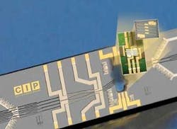
The technique integrates optics in a way similar to mounting electronic printed-circuit boards (PCBs) on a motherboard. Developed and refined over a period of ten years, it has been optimized for low interface losses and ease of assembly, and does not involve any complex processing or etching. The technique is also highly scalable and applies equally well to two devices or a large subsystem integrating many component elements. Systems require only passive assembly, saving cost and time. The technique also offers ways of harnessing new optical functionalities. Within two years, CIP expects to be producing systems with new functionality that can only be technically achieved with systems built using its new rationale.
Graeme Maxwell, CIP’s vice president of hybrid R&D, explains that traditionally the research departments in companies producing semiconductor devices, such as lasers or amplifiers, focused their efforts on the indium phosphide (InP) chip and worried about the packaging later. Requiring highly skilled labor, packaging involves complicated optical alignments, as well as physically boxing the chip, and is usually outsourced to the Far East. The development team at CIP, originally as part of British Telecommunications (London, England) and then Corning (Corning, NY), started with a broader perspective-designing a chip for manufacture.
“This meant taking into account not just the chip, but all the stages through to packaging,” says Maxwell. “And there are modifications that you can make to the chip that allow the packaging to be simplified.”
These modifications include changing the optical mode in the chip. Usually an InP chip has a small mode, leading to strong diffraction, which in turn makes it necessary to use a more complex coupling scheme such as lens-ended fibers. Researchers at CIP have increased the optical mode size to simplify the optical alignment, and have also concentrated on precision machining-having clean, well-defined cleaved faces combined with precise mating components that make physical alignment easier. Added together, these modifications become a new manufacturing concept, the photonic analog of the electronic motherboard-daughterboard structure.
Silica motherboard
The CIP “motherboard” is based on planar silica, with the daughterboards being based on micromachined silicon submounts. Physical features on both types of board and on the chips themselves allow easy and exact location of chip and boards in the final system. And the large optical-mode size makes alignment less critical. “Assuming the fabrication tolerances are within spec, then everything can just be dropped in,” explains Maxwell. “It’s not quite like stuffing electronic PCBs yet, but in the future we will get close.”
In CIP’s commercial 2R regenerator, the component integrates a planar silica Mach-Zehnder interferometer and a monolithic quadruple semiconductor-optical-amplifier array to create a dual-channel regenerator with just a 1 dB loss at daughterboard-motherboard interfaces.
Maxwell says other companies are moving in the same direction, as scalability becomes an issue. His own group is looking at pushing the technology further, including as part of European collaborative work. He expects to offer systems that rely on optical functions, such as stable and temperature-insensitive time delays, that cannot be robustly provided by existing technologies.
“We believe this hybrid integration technique provides the performance, reliability, and economy to address many of the sophisticated component functions necessary for advanced optical switched fabrics,” he says. “Among the potential applications are reconfigurable add/drop multiplexers, 2R and 3R signal regenerators, high-speed interconnects, packet switches, WDM PON (wavelength-division-multiplexing passive-optical-network) devices and optical buffer memories. In each of these cases, I expect our platform approach to offer considerable cost reduction and performance advantages over current component solutions and integration methods.”
