Improving the stability and imaging time of TERS
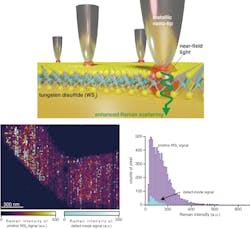
Researchers in Japan have improved an optical nanoimaging technique called tip-enhanced Raman spectroscopy (TERS) to improve the spatial resolution and stability of large micrometer-sized samples. They demonstrated the technique on tungsten disulfide (WS2) film, a coating commonly used in industrial applications for its properties of lubrication and durability. The new method uses a laser-guide-beam feedback system to stabilize both the position of the focal point and a metallic imaging nanotip used to confine the light field on the sample.
To study the active materials used in ever-smaller devices, such as those used in optoelectronics, long-duration TERS is a necessity. Researchers must evaluate entire sample areas measuring a few microns for irregularities, defects, and chemical composition. The technique is indispensable for characterizing chemical and optical properties in numerous nanotechnology applications, such as in detection of tiny defects in 2D coatings. But long-time, large-area, high-resolution conventional TERS imaging has long been a challenge. Surveying an area larger than a square micron is difficult, because the imaging system drifts in less than a second.
Raman imaging is a notoriously weak process. The TERS technique requires the imaging nanotip to coincide with the center of the focal spot of the excitation laser, which excites the surface of the 2D material via plasmon resonance. The surface plasmon resonance enhances the Raman signal of the sample to enable detection of enough photons for measurable imaging. Without a stable nanotip coinciding with a steady focal point, the imaging is limited to only a few hundred milliseconds. This limits the size of the sample that can be scanned; a single scan of a 1 µm2 sample would take a minimum of 30 minutes.
Ryo Kato, assistant professor at the Institute of Post-LED Photonics at Tokushima University (Osaka, Japan), and colleagues found a way to overcome these long-standing tradeoffs between imaging time, imaging area, and resolution. Kato himself had been suffering the drift inherent in TERS microscopy while attempting to evaluate 2D WS2 samples for use in optoelectronic devices (see figure). Unlike graphene, WS2 has a bandgap that enables its versatile application in photodetectors, transistors, and photovoltaic devices. But the performance of the film can be degraded by random structural defects, so it’s important to identify and understand them.
Long-time, ultrastable TERS
A few groups were attempting to tackle the drift issue, but were unable to achieve long-time TERS imaging that compensated for the thermal and vibrational drift of both the focal point and the nanotip. To address the problem, a research team composed of Kato and professors Takayuki Umakoshi and Prabhat Verma of Osaka University developed a laser feedback system much like those used in astronomical observatories, which compensate for poor atmospheric conditions. The team used a 488 nm Sapphire SF NX guide laser from Coherent (Santa Clara, CA), beaming at a high incident angle through the imaging system, joined by a lateral position detector from Thorlabs (Newton, NJ) and a piezo-controlled objective scanner from nanoFaktur (Villingen, Germany), to track, maintain, and correct the position of the nanotip with respect to the focal point.
This method uses the guide laser and the lateral position detector to sense the displacement of the laser focus. The piezo galvo-scanners image the laser spot around the nanotip just as it approaches the WS2 layer, obtaining a Rayleigh scattering image. The detected position travels in a feedback loop through the piezo controller, which compensates for the focal drift to within ±5 nm. The exposure time for each image takes approximately a third of a second, with step sizes ranging from 10 nm to 195 nm—the sub-nanometer spatial resolution required to detect defects in WS2 layers without any significant loss of optical signal.
The team was able to image a 1 × 4 µm sample over six hours of stable imaging, a 12x improvement in the imaging duration over conventional TERS imaging. The team notes in their paper in Science Advances that the ultrastable system theoretically has no limit on imaging time, except perhaps oxidation of the tip. The technique revealed new nanoscale protrusions in the WS2 monolayer. Was it oxidation, they wondered? Rather, the hyperspectral information obtained using the technique enabled the team to conclude that the protrusions were small metallic grains formed during substrate fabrication.
“Raman spectroscopic imaging of large-sized tungsten disulfide at the nanoscale allows us to unveil not only remarkable physical, optical, and chemical properties of nanomaterials for optoelectronic devices, but also to characterize the performance and quality of the devices themselves,” says Kato.
The new ultrastable TERS imaging technique could enable discovery of new nanoscale heterogeneities while spectroscopically characterizing them in a plethora of applications. In addition to optoelectronic devices, the method has commercial potential in all kinds of nanostructured materials, such as those in semiconductor fabrication, polymers, aerospace, military, medicine, and optoelectronic devices.
The next step is to improve temporal resolution. “If the imaging speed can be improved, we can perform nanoimaging of further large-sized samples, scaling to a few hundred microns,” says Kato.
The hope is to apply the technique to precise, high-resolution imaging of biological samples. According to Kato, fast enough imaging would make it conceivable to achieve continuous monitoring of the biological dynamics in molecules.
About the Author

Valerie Coffey-Rosich
Contributing Editor
Valerie Coffey-Rosich is a freelance science and technology writer and editor and a contributing editor for Laser Focus World; she previously served as an Associate Technical Editor (2000-2003) and a Senior Technical Editor (2007-2008) for Laser Focus World.
Valerie holds a BS in physics from the University of Nevada, Reno, and an MA in astronomy from Boston University. She specializes in editing and writing about optics, photonics, astronomy, and physics in academic, reference, and business-to-business publications. In addition to Laser Focus World, her work has appeared online and in print for clients such as the American Institute of Physics, American Heritage Dictionary, BioPhotonics, Encyclopedia Britannica, EuroPhotonics, the Optical Society of America, Photonics Focus, Photonics Spectra, Sky & Telescope, and many others. She is based in Palm Springs, California.