A robust new telecom qubit in silicon
Quantum technologies are expected to transform computing, communication, and sensing by harnessing the unusual behavior of matter at the atomic scale. Translating quantum’s promise into practical devices will require physical systems that have desirable quantum properties and can be easily manufactured. Qubits (quantum building blocks) based on superconducting circuits have been made into operational quantum computers, but the size of the equipment and the complicated fabrication processes and operation remain a challenge to make such computers scalable. On the other hand, silicon, the material behind today’s computer chips, is highly attractive as a platform because it plays to the strengths of the existing trillion-dollar semiconductor industry. It makes identifying qubits in silicon an important frontier research area.
Qubits can be based on atomic-scale defects within a crystal. A prototype example is the nitrogen-vacancy (NV) center, which consists of a nitrogen (N) atom sitting next to a vacancy (V, a missing carbon atom) within a diamond crystal. These defects can interact with both electrons and light, which allows them to emit single photons (quanta of light) that can transmit quantum information or be processed in quantum networks.
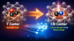
Silicon has gained interest as a host material for defect qubits, because—unlike in the case of diamond—the mature fabrication and processing of silicon will allow scalable production of quantum computers and networks. Our team at the University of California, Santa Barbara recently identified a robust new qubit in silicon as a promising alternative to the T center, a silicon qubit already being heavily pursued (see Fig. 1).
The T center in silicon for quantum information applications
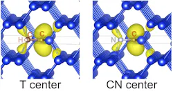
Much recent work has focused on the T center, a silicon defect made of carbon and hydrogen atoms (see Fig. 2, left) that can store quantum information for long periods of time, comparable to coherence times within an NV center (milliseconds). The quantum information is stored in both the electron spin (due to an unpaired electron) and the nuclear spin of the hydrogen. It also emits light within the telecom O-band, with an experimentally measured zero-phonon line (ZPL) of 935 meV (1326 nm). But the presence of hydrogen (H) within the T center renders it fragile and sensitive to fabrication conditions. Hydrogen can easily move within the crystal and is difficult to control during processing, which makes reproducible and reliable device manufacturing challenging to achieve.
CN center: A more robust silicon defect
Our team identified a promising alternative to the T center: the CN center, which consists of carbon (C) and nitrogen (N) atoms (see Fig. 2, right). The CN center is chemically similar to the T center because N has the same number of protons and electrons as C+H. Like H, N also has non-zero nuclear spin. Because the CN center does not contain H, it will be more robust and easier to achieve in actual devices.
We used advanced first-principles computer simulations to model the defect at the atomic level. These simulations allow us to predict material properties of new systems that have not yet been realized experimentally, and they help guide future efforts to engineer and fabricate novel devices. Specifically, we used density functional theory with state-of-the-art hybrid functionals to accurately predict the stable atomic structures and the corresponding electronic structures of the defects.
We modeled the system by putting up to 1,000 silicon atoms into a simulation box called a “supercell,” and placed the defect atoms accordingly. It turns out, the CN center is stable against decomposition into C and N substitutional and interstitial defects. We also showed that the CN center reproduces the key electronic and optical properties that render the T center attractive for quantum applications. Like the T center, the electronic excited state corresponding to the ZPL transition involves a bound exciton whose spatial range spans beyond the simulation cell sizes that are computationally tractable. To handle this challenge, we developed a new method to extrapolate the excitonic properties from calculations performed in computationally tractable cells, which allows us to reliably calculate the optical properties. We predict a ZPL of 828 meV (1498 nm) within the telecom S-band.
Identifying a hydrogen-free, telecom-wavelength quantum-light emitter in silicon is an important step to bridge the gap between quantum science and scalable technology. The CN center could serve as a practical new building block for quantum devices to potentially accelerate the development of advanced quantum technologies while using the same silicon material that powers today’s electronics.
Funding for this research was provided by the Department of Energy Office of Science, Office of Basic Energy Sciences, through the Co-design Center for Quantum Advantage (C2QA).
FURTHER READING
J. K. Nangoi, M. E. Turiansky, and C. G. Van de Walle, Phys. Rev. B, 113, L060101 (Feb. 10, 2026); https://doi.org/10.1103/zy5b-fskh.
About the Author
J. Kevin Nangoi
J. Kevin Nangoi is a postdoctoral researcher at the University of California, Santa Barbara.
Mark E. Turiansky
Mark E. Turiansky is a postdoctoral researcher and Quantum Foundry Fellow at the University of California, Santa Barbara.
Chris G. Van de Walle
Chris G. Van de Walle is a distinguished professor and the Herbert Kroemer Chair in Materials Science at the University of California, Santa Barbara. He is also a principal investigator in the Co-design Center for Quantum Advantage, and a Thrust co-leader in the UC Santa Barbara Quantum Foundry.