Optical and electrical control of a silicon-based quantum device?
A new diode nanocavity created by a team of researchers at Simon Fraser University (SFU) and quantum company Photonic Inc. in Canada enables optical and electrical control of silicon “color center” qubits. Until now, these qubits, a.k.a. T centers, were controlled optically with lasers. This dual control option of T centers hints at potential applications for future scalable quantum computers (see video).
The microelectronics industry is rising to the challenge of developing silicon nanofabrication and ever-smaller transistors to meet the insatiable demand for computational power. It’s led to an enormous collection of knowledge about how to purify and process silicon to create extremely small devices—and silicon is now a versatile platform that can host both electronic and photonic devices.
“Mike Thewalt and Stephanie Simmons, the founders of the Silicon Quantum Technology lab at Simon Fraser University and Photonic Inc., were studying impurities within isotopically purified Si-28 (an isotope of silicon) and discovered these impurities have long spin coherence times that can make them useful for quantum applications,” says Michael Dobinson, a Ph.D. candidate in physics at SFU.
Then they searched for a luminescent defect, a “color center,” within silicon to act as a spin-photon interface—a quantum system that can store quantum information within a spin state and distribute quantum information through emitted photons. In 2020, they identified the T center, which has excellent spin properties, emits within the telecommunications O-band, and enables low-loss transmission over standard optical fibers.
During this time, development of other quantum computing platforms was underway across a range of modalities. A range of color centers were explored for solid-state platforms, including diamond and silicon carbide, and it turns out their capabilities can be extended by controlling the electronic environment—including its electrical excitation, charge depletion, and spin-charge readout.
“In 2022, our group developed silicon nanophotonic devices that allowed us to control single T centers optically with lasers,” says Dobinson, who has a background in electrical engineering and is interested in single-photon sources and optically active quantum defects. “Adding electrical control has the potential to unlock new capabilities, which made it intriguing for us to explore for the T center. We used industry-standard tools and processes to design and fabricate our devices.”
For his Ph.D., Dobinson wanted to work on quantum technology and he focused on whether it can scale. “Coming from engineering and seeing the requirements for quantum computing, I knew it was the most important metric,” he says. “I researched all modalities and eventually started in the Silicon Quantum Technology lab at SFU in 2022. After discussions with Stephanie Simmons and Daniel Higginbottom, now both assistant professors in physics at SFU, I saw the potential for integration of the T center with both optical and electrical controls as an exciting crossover between everything that interests me and as an important component for scalability.”
T centers
The team’s work involves several different optical and electrical components and a wide range of concepts that are helpful to understand.
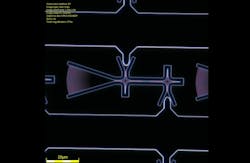
For starters, the nanocavity device they used for their single-photon emission demonstration is based on a T center, a color center within silicon that’s a quantum emitter. It consists of two carbon atoms and a hydrogen atom, which take the place of a silicon atom.
“The T center hosts a ground state electron spin and a bound-exciton excited state that has an optical transition within the telecommunications O-band ~935 meV (1326 nm),” Dobinson explains. “This device’s T centers are within an optical cavity—a nanophotonic device that consists of a waveguide with a periodic array of holes. It creates a photonic crystal cavity to enhance the interaction between the T center and optical field by the Purcell effect, which causes an increased spontaneous emission rate into the cavity mode that results in brighter emission from the T center. The Purcell effect scales by Q/V, where Q is the quality factor of the cavity and V is the mode volume.”
T centers within the device can be excited electrically by the p-i-n diode, which is formed across the cavity. This diode is created by doping one side of the device with phosphorus to create an excess of electrons, and doping the other side with boron to create an excess of holes. “It creates a built-in potential that, when overcome by a forward-biased electrical voltage, allows charge carriers to be injected into the central region of the device,” Dobinson says. “T centers within the central undoped region can capture these free carriers to add energy to the system and take it to an excited state. Upon recombination, the T center emits light.”
The emission from the T centers coupled into the cavity is routed by a waveguide that confines the light to a mode that’s directed around the photonic chip. “It relies on the refractive indices of the waveguide and surrounding material. We use silicon-on-insulator, which has a high-index silicon layer with a low-index oxide layer on the bottom,” says Dobinson.
After routing the emission by the waveguide, it’s directed out of plane into an optical fiber by a grating coupler. “This consists of a periodic array of etches within the silicon to create a periodic variation in the effective refractive index, which causes reflection and refraction from each interface,” Dobinson says. “It directs the waveguide mode out of plane into the mode of the optical fiber positioned above, with some coupling loss.”
To determine whether T centers can be used as an electrically injected single-photon source requires collecting single photons. “To do it, we perform a Hanbury-Brown-Twiss measurement, in which we measure the second-order correlation function, g(2)(0). This takes the incoming stream of photons and directs it into two branches to record the photon arrival times,” Dobinson says. “For a true single-photon source, there should never be two photons at a time—so the detectors will not record simultaneous photon arrivals. By analyzing the data, we can look for correlations, instances where both detectors recorded photons, for different time delays. We can confirm that the emission is predominantly from a single-photon source if at zero delay g(2)(0) < 0.5.”
The team also explored spin initialization. “We consider the T center’s behavior as a spin-photon interface,” Dobinson adds. “Under a magnetic field, we see four optical transitions from the T center—each with different energy that corresponds to the initial and final spin state of the T center. To initialize the spin state of the T center, we filter for photons with the energy corresponding to an optical transition to that spin state. When we detect a photon that passes through our filter, we know it had a specific energy and that the T center is in a specific spin state, with some fidelity.”

Setup—keep it cool
The team’s method involves applying an electrical pulse to the p-i-n diode, which injects free carriers into the device. And the device’s T centers capture the free carriers to enter an excited state. “Upon recombination, the T center emits a photon that’s coupled to the cavity mode,” says Dobinson. “The rate of recombination is also enhanced by the optical cavity.”
A photon is sent through a waveguide to a grating coupler that couples the light out of the chip and into an optical fiber. The light is then filtered to isolate emission from a single T center, which can then be used as a single-photon source. Its energy is also correlated to the spin state of the T center under a magnetic field, which allows the researchers to apply electrical pulses until they measure a photon of the correct energy that corresponds to the spin state they want to prepare.
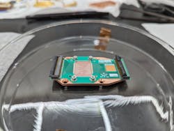
Their setup uses a cryostat to keep the chip cooled to 1.5 K. “The chip is mounted to 3-axis cryogenic nanopositioners, which are used to couple to the devices optically by an optical fiber array above the chip,” Dobinson says. “The chip is also wirebonded to a printed circuit board to route the electrical connections off the chip by flat-flex ribbon cables. Outside of the cryostat, we use a fiber Fabry-Perot cavity and free-space filters to filter the emission.”
Future devices could integrate this type of filtering onto the chip itself. And finally, the filtered emission is detected by a superconducting nanowire single-photon detector (SNSPD), which is cooled to 0.8 K.
Aha!
Design and fabrication of the chip took months, during which Dobinson was working on the measurement apparatus and design of the experiments. “The first time I held the actual chip and looked at the nanostructures under a microscope was very exciting—it was incredible to see just how intricate the devices were,” he recalls. “After cooling down the chip within the cryostat, it was also exciting to apply a forward bias to a device for the first time and see luminescence and confirm by spectroscopy it was indeed from T centers.”
An “aha!” moment struck while Dobinson wondered what would happen with emission within a magnetic field. “I wasn’t thinking much about spin initialization at the time,” he says. “I had a single laser, so it wasn’t feasible to measure the center using the usual optical methods—and then I realized the electrical excitation could ‘repump’ the ground state population and use the laser to probe the four optical transitions.” This set in motion the spin initialization concepts.
What does the team’s work mean for nanophotonics and PICs?
For the realm of nanophotonics and photonic integrated circuits (PICs), there’s an effort underway to develop electrically injected single-photon sources. “Often, these devices rely on heterogeneous integration—combining silicon photonics with other materials—for electrically injected on-chip light sources,” says Dobinson. “An on-chip light source native to silicon is compelling because it may simplify integration. The devices we demonstrate can also feasibly be adapted to other silicon color centers that don’t have a comparable spin-photon interface, but may have advantages for these classical applications.”
As far as quantum applications, dual electrical and optical control may enable many applications beyond being a source of single photons. “We’ve demonstrated that it can be used for spin initialization, and the electrical interface and small footprint of these devices can enable fast and highly parallel control,” Dobinson adds. “Our work in other platforms shows that controlling the electronic environment can improve the spectral and spin properties of quantum emitters. Combining the electrical and optical control with nanophotonic devices enables scaling up to larger systems of quantum emitters on a single chip. We’d like to explore the wide range of applications for these hybrid nanophotonic/p-i-n diode devices to develop the T center for quantum computing applications.”
Challenges and improvements ahead
The devices involved in this work are first generation, so Dobinson and colleagues already have a few improvements in mind.
“This first chip has many devices connected in parallel, which limits the number that can be controlled individually,” Dobinson explains. “We also performed the filtering off-chip, but future devices can potentially bring it onto the chip. Scaling the number of devices will require work to route the electrical connections. Developing fabrication processes compatible with the electrical and optical components, as well as the T center itself, will continue to be an engineering challenge. And scaling these types of devices for a larger quantum system will also require high yield. Photonic Inc. is already working to scale up T center devices for quantum computing applications.”
What’s next? The team is exploring other possible modes of operation for these devices. “We can excite the T center under forward bias, but by applying a reverse bias we expect that we can tune the emission energy by the Stark effect,” says Dobinson. “We’d also like to explore the effects of charge depletion of the spectral and spin properties of the T center. These are the main goals of my current research, and we’re also planning the next generation of these devices to improve the efficiency, yield, and addressability.”
FURTHER READING
M. Dobinson et al., Nat. Photon., 19, 1132–1137 (2025); https://doi.org/10.1038/s41566-025-01752-8.
About the Author

Sally Cole Johnson
Editor in Chief
Sally Cole Johnson is Laser Focus World’s editor in chief, and she has more than 25 years’ experience as a science and technology journalist. She specializes in physics and semiconductors, and wrote for the American Institute of Physics for more than 15 years, and also covered theoretical physics and neuroscience for the Kavli Foundation, and complexity for the Santa Fe Institute. Johnson has also written extensively about military embedded systems, high-performance computing, software-defined networks, and infosec.
When she isn’t writing about optics, photonics, or quantum advances, you can find her outside in northern NH in the garden with birds landing in her hand or heading for the mountains with her bike, skis, or crampons and ice axe.