Tailor-made, large nonlinearities within nanophotonic devices?
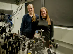
A multiquantum well (MQW) material created by Seth Bank, a professor of electrical and computer engineering, and his group at The University of Texas at Austin shows potential for nonlinear photonics applications. These engineered semiconductor heterostructures caught the attention of Pernille Undrum Fathi, a Ph.D. candidate in Federico Capasso’s group at Harvard University, and colleagues because their electronic structure can be designed to create a tailor-made nonlinear response at desired wavelengths.
As with bulk materials, researchers are searching for a way to efficiently access nonlinear properties—and for these semiconductor heterostructures, the strongest nonlinear response is difficult to access from free space. Working with Marcus Ossiander, a professor at the Technical University of Graz in Austria, Fathi and colleagues developed a metasurface approach to access this nonlinear response.
“We were inspired to combine this material with metasurfaces because it enabled devices where we control the light-matter interaction at multiple levels—from how the light distributes and behaves within the material using metasurfaces to how it interacts with electrons through the design of coupled quantum wells,” she says. “In combination, it yields a huge, tunable, and free-space-accessible second-order optical nonlinearity.”
It starts with a MQW material
Fathi and colleagues’ work starts with the MQW material developed and grown by Seth Bank’s group. “They use molecular beam epitaxy to grow nanometer-scale layers of different semiconductor materials and create asymmetric coupled quantum wells,” she says. “By carefully choosing the composition and thickness of these layers, we can engineer the electronic energy levels of the material and its nonlinear optical properties.”
Established nonlinear quantum well approaches tend to rely on transitions between energy levels with the conduction band, which can enable extremely strong nonlinearities. “But the photon energies we can reach are limited by the conduction band offset of the materials, so this approach is predominantly used at mid-infrared wavelengths,” she says. “Instead, we use transitions between the valence and conduction bands to allow us to extend the concept to much higher photon energies—including near-infrared wavelengths used for telecommunications, with a route toward the visible part of the spectrum.”
Electron transitions within the material are governed by selection rules that determine which polarizations must be present. “For the interband transitions we use, the result is a material with very good nonlinear properties—but it’s difficult to access these properties when illuminating the material from free space,” says Fathi.
By combining it with metasurfaces, which are engineered arrays of nanostructures with sub-wavelength spacing, “we can tailor the electromagnetic field response so that the light is able to drive the interband transition within the material,” she says. “The metasurface introduces a resonant mode with high field intensity and the correct polarizations, which enables good access to the nonlinear properties of the material.”
How does the metasurface work?
The metasurface works like a grating coupler to a waveguide. “We pattern an array of nanoscale titanium dioxide (TiO2) pillars atop the nonlinear material,” Fathi explains. “This periodic structure redirects the incoming light into the high refractive index film, where it’s reflected at the interfaces due to total internal reflection. If the light accumulates the correct round trip phase it becomes coupled to a resonant guided mode, which allows the field to build up within the nonlinear material before being out-coupled by the same nanostructures.”
The resonant mode the researchers couple to has electric field components both parallel and perpendicular to the quantum well layers to allow it to access the nonlinear tensor element of their material, which requires orthogonally polarized field components. “In other words, the metasurface provides two key things: It converts the polarization of the incident fields to match what’s needed to access the nonlinearity, and it resonantly enhances the fields to make the nonlinear interaction stronger,” she says.
Working with a new material brings along uncertainty and, unlike off-the-shelf materials, it tends to lead to shifts in the optical response and larger mismatches between simulations and experiments. “The high quality factor of the resonances made resolving it in linear measurements difficult,” Fathi says. “For a long time, we were relying entirely on the nonlinear signals to validate our measurements against simulations.”
Experimental work comes with its own challenges. “It requires a range of different areas of expertise, as well as fabrication and characterization facilities, so our samples are well traveled,” she says. “The material is grown by Seth Bank’s group at The University of Texas at Austin, characterized by Xiaoqing Pan’s group at the University of California, Irvine, and substrate transferred by Igal Brener’s group at Sandia National Laboratories, before finally arriving at Harvard, where we fabricated the metasurface and characterized the material and combined the metasurface-heterostructure device. This is an interdisciplinary project combining materials science and semiconductor physics with nanophotonics. Bridging the gaps in understanding so everyone speaks the same language when codesigning components of the final device was a key part of this large collaboration.”

Symmetry breaking
A need for symmetry breaking was the most surprising part of the work for Fathi. The group initially expected designing a strong resonance and maximizing the relevant fields would result in the nonlinear enhancement they wanted.
“Instead, we realized that at perfectly normal incidence the nonlinear contributions generated across the structure cancel each other,” she says. “Returning to the simulations and analytical descriptions of transverse magnetic guided modes, we realized this comes down to a fundamental symmetry of the system causing the nonlinear contributions to cancel in the symmetric normal incidence case—and enabling it the moment symmetry is broken by tilting the sample by a tiny amount.”
Stronger nonlinear interactions
Nonlinear optics enables generation of light at new frequencies where suitable lasers might not be available, ultrafast and all-optical signal processing, and generation of entangled photon pairs for quantum computation and communication.
The group’s work demonstrates a path toward stronger nonlinear interactions within devices with very small footprints. “It can enable increasingly compact photonic devices for both classical and quantum applications, as well as new functionalities in cases where the available input signals were previously too weak to efficiently drive nonlinear processes,” says Fathi.
On the horizon: More tailoring
Fathi and colleagues see several directions they’re excited to pursue now, but emphasize this is still fundamental research and there’s work to do to better understand and optimize both the MQW materials and metasurfaces. “The individual fabrication techniques used for our work are well established, which provides a promising foundation for eventually translating these devices beyond university cleanrooms,” she points out.
The flexibility of interband resonant structures “opens the door to tailored nonlinear materials operating at even higher photon energies, including the visible,” Fathi says. “There are many degrees of freedom to design that weren’t used in this first demonstration that may enable new functionality at the device level. Seth Bank’s group also recently published a paper in Optica1 about how the material itself—including details about the growth and design—could lead to even larger nonlinearities.”
On the metasurface side, the researchers barely scratched the surface when it comes to the freedom these structures provide to tailor their electromagnetic field response. “Multiresonant structures or devices that independently engineer the phase of the fundamental and second-harmonic fields come to mind,” Fathi says. “The extreme sensitivity to symmetry we demonstrated could also provide an interesting route toward highly sensitive devices. Finally, we’re interested in exploring these materials for further frequency mixing processes, such as spontaneous parametric downconversion to generate entangled photon pairs.”
FURTHER READING
P. U. Fathi et al., Nat. Nanotechnol. (2026); https://doi.org/10.1038/s41565-026-02268-0.
REFERENCE
1. R. Ramesh et al., Optica, 13, 9, 1854–1860 (2026); https://doi.org/10.1364/optica.605894.
About the Author
 Sally Cole Johnson
Sally Cole Johnson
Editor in Chief
Sally Cole Johnson is Laser Focus World’s editor in chief, and she has more than 25 years’ experience as a science and technology journalist. She specializes in physics and semiconductors, and wrote for the American Institute of Physics for more than 15 years, and also covered theoretical physics and neuroscience for the Kavli Foundation, and complexity for the Santa Fe Institute. Johnson has also written extensively about military embedded systems, high-performance computing, software-defined networks, and infosec. She is a member of the National Association of Science Writers (since 2001).
When she isn’t writing about optics, photonics, or quantum advances, you can find her outside in northern NH in the garden with birds landing in her hand or heading for the mountains with her bike, skis, or crampons and ice axe.