Reliable monitoring of optical coating deposition processes is key to complex thin film elements
In light of today’s outstanding capabilities for designing the most complex types of optical coatings1-3 and the diversity of modern deposition processes to produce these coatings, reliable monitoring of optical coating production has become a critical challenge for the further development of the most complex thin film optical elements. To respond to this challenge, various types of optical monitoring techniques can be used.
Features of optical monitoring
The most important feature of optical monitoring techniques is the ability to track the optical thicknesses of coating layers. Spectral properties of optical coatings are determined by the interference effects within the coating structure, which depend on the optical, rather than physical, thicknesses of the layers. Even with the best deposition processes, small deviations of layer refractive indices from their nominal values are inevitable, because they are caused by small fluctuations in the density of the deposited layers. Optical thickness monitoring automatically adjusts the physical thicknesses to keep the primary parameters close to the nominal values.
Another notable feature of optical monitoring is the potential existence of the error self-compensation effect. It is important to emphasize that the primary goal of monitoring is not to reduce layer thickness errors but to achieve high accuracy in the spectral characteristics of the produced multilayer coating. Thanks to the error self-compensation effect, high accuracy can be achieved—even with significant thickness errors.
Correlation of errors by optical monitoring
The error self-compensation effect results from the correlation of errors in layer thicknesses by an optical monitoring procedure. In the case of direct optical monitoring on a sample, the thickness errors of all previously deposited layers affect the monitoring signal of the currently deposited layer, which results in a correlation of thickness errors across all layers of the deposited coating. If a monitoring procedure with multiple witness chips is used, the correlation occurs within the layers monitored by each chip.
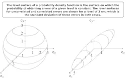
We can consider thickness error vectors composed of errors in individual layers. These vectors are elements of an m-dimensional space, where m is the number of coating layers. Error analysis is a statistical analysis that considers multiple error vectors of different nature. If we consider uncorrelated thickness errors, they are uniformly distributed in m-dimensional space, and the level surfaces of their probability density function are spheres in this space. Correlated thickness errors are unevenly distributed and have certain preferred directions in this space (a 3D example is shown in Fig. 1).
Error self-compensation effect
Quality of the produced optical coating can be assessed using a merit function (MF), which represents the standard deviation of the coating’s spectral characteristics from the target characteristics. The MF reaches its minimum for the theoretical coating design and has positive variations if there are errors in the thicknesses of this design.
Self-compensation of errors occurs if the variations of MF in the preferred directions of correlated errors are minor. The strength of the error self-compensation effect is assessed by the ratio of the mean MF variations calculated for ensembles of correlated and uncorrelated thickness errors. The error levels in these ensembles should be identical—and the smaller this ratio the stronger the effect.
Variety of optical monitoring techniques
A wide range of optical monitoring techniques are currently used. The main subdivision is broadband and monochromatic monitoring. A familiar type of monochromatic monitoring called “turning point monitoring” was discovered more than 50 years ago4 and occupies a special place due to its remarkable property. This type of monitoring provides a strong error self-compensation effect. Unfortunately, turning point monitoring is only applicable to one class of optical coatings: Coatings with quarter-wave and multiple quarter-wave layer optical thicknesses. Furthermore, strong error self-compensation effect is observed only for narrow pass-band filters with such layers.
In recent years, it has become clear that the error self-compensation effect also occurs in broadband and monochromatic monitoring of coatings with non-quarter wave layer optical thicknesses. Selecting the correct monitoring procedure for a given type of optical coating can allow this effect to be exploited in the manufacturing process. This is demonstrated using the example of a complex narrow pass-band filter with arbitrary layer thicknesses. For the filter in question, monochromatic monitoring using four changeable witness chips, with multiple monitoring wavelengths per chip, proves advantageous due to the presence of a very strong error self-compensation effect.5
Challenging narrow pass-band filter
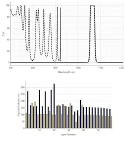
The transmittance of a filter with a pass-band region centered at 1064 nm is shown at the top of Figure 2. Typically, pass-band filters with steep transmittance slopes are designed as Chebyshev-type multicavity filters with quarter-wave layer optical thicknesses, because these filters allow for turning point monitoring. Unfortunately, filters of this type can’t provide the required width of the high reflection zone to the left of the pass-band region. This is why a more complex 59-layer filter with non-quarter wave layer optical thicknesses is required.
Simulation experiments on filter production
Numerous random factors can cause errors in the thicknesses of deposited coatings. Therefore, a monitoring technique’s applicability for a specific coating can be assessed through statistical analysis of multiple simulation runs. The results of an analysis of the 59-layer narrow pass-band filter when using monochromatic monitoring with four witness chips are shown in Figure 3, and are based on 1,000 simulation experiments. Many experiments are required to obtain reliable statistical results, and the cumulative distribution functions in Figure 3 show the probability of obtaining MF variations less than the value indicated on the abscissa.
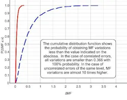
The probability of obtaining small MF variations in the case of correlated thickness errors is significantly higher than in the case of uncorrelated errors, and this is a direct consequence of the strong error self-compensation effect. Mean MF variations in the former case are nine times smaller than in the latter.
By selecting an appropriate monitoring technique and using the error self-compensation effect, these types of filters are now successfully being manufactured.
REFERENCES
1. J. D. T. Kruschwitz, “Software tools speed optical thin-film design,” Laser Focus World, 39, 6, 157–166 (2003).
2. J. D. T. Kruschwitz, “Software drives development of a ‘perfect’ interference coating,” Laser Focus World, 47, 7, 33 (2011).
3. A. Tikhonravov, Optical Coatings: design, characterization, monitoring (SPIE, 2024).
4. H. A. Macleod, “Turning value monitoring of narrow-band all-dielectric thin-film optical filters,” Optica Acta, 19, 1–28 (1972).
5. A. V. Tikhonravov, S. A. Sharapova, and S. K. Kirpichenko, “Monochromatic monitoring of optical coatings production using multiple witness chips,” Numer. Methods Program., 27, 3, 514–522 (2026); doi:10.26089/nummet.v27r332.
About the Author
Jennifer Kruschwitz
Jennifer Kruschwitz is an Associate Professor of Optics, Director of the Robert E. Hopkins Center for Optical Design and Engineering, Co-Chair of the Optics Master’s program, and Senior Scientist at the Laboratory for Laser Energetics at the University of Rochester. She received her BS and MS in Optics from the University of Rochester, and her PhD in Color Science from Rochester Institute of Technology. She is author of the Field Guide to Colorimetry and Fundamental Color Modeling (SPIE Press). She is a Senior Member of SPIE and a Fellow of Optica.
Alexander Tikhonravov
Alexander Tikhonravov is Professor of Theoretical Physics, Lab Head, and Research Supervisor at the Research Computing Center of M. V. Lomonosov Moscow State University. He received his Ph.D. and Doctor of Sciences degrees in physics and mathematics from Moscow State University. He has authored over 450 publications, including Optical Coatings: Design, Characterization, Modeling (SPIE Press). He is the inventor of the needle optimization technique, a universal tool for designing modern optical coatings. He is a Fellow of Optica.