Organic thin film brings second-order optical nonlinear effects to silicon photonics
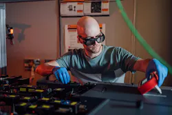
In an advance for photonic integrated circuits (PICs), Stéphane Kéna-Cohen and his team at Polytechnique Montréal in Canada recently fabricated waveguides for frequency doubling using an organic thin film—based on triphenylamine-dicyanoquinoxaline, a.k.a. TPA-QCN—that strongly interacts with light (see video). This class of materials may help lessen AI’s energy load on data centers because it can be placed onto silicon to process light directly and eliminates converting electric and photonic signals back and forth.
TPA-QCN is deposited via vacuum evaporation to form a layer of molecules that spontaneously adopt a preferred orientation. This alignment provides it with a second-order optical nonlinear response, which means light beams can interact while passing through it.
“We were inspired by beautiful work being done within an entirely different field—organic light-emitting diodes (OLEDs) for displays,” says Kéna-Cohen, a professor of engineering physics, as well as the Canada Research Chair in Light-Matter Photonics. “Researchers realized that certain classes of molecules automatically align during fabrication. In their case, this leads to the buildup of a voltage that typically hurts device performance. This voltage buildup, which requires polar molecules to orient along a preferential direction, was the first sign that we should be able to use similar materials for nonlinear optics.”
Second-order nonlinear photonic devices ahead
Silicon is the dominant platform for integrated photonics today, but it’s not good for fabricating modulators and amplifiers. “One ingredient silicon lacks to make good modulators is the Pockels effect, which allows a direct-current electric field to interact with an electric field at optical frequencies—and it’s a good example of a second-order nonlinear optical effect,” explains Kéna-Cohen. “Parametric amplifiers and oscillators rely on second-order nonlinearities. For these types of effects, engineers need to use other materials such as lithium niobate either as standalone components or go through the complex process of integrating the two.”
Another concept involved in the design of second-order nonlinear photonic components is a phase matching requirement—the phase velocity of the interacting light waves needs to match to avoid destructive interference effects. “Unfortunately, the fact that all materials have dispersion automatically prevents this, so clever tricks need to be used for phase matching. In lithium niobate, a common approach is to use electrodes along the propagation direction to flip the domain orientation—a.k.a. electric field poling.”
Advantages: Deposited on-chip directly, birefringence
The team’s approach brings two key advantages. “First, our organic thin films can be deposited directly onto any chip by using standard dry fabrication processes—without worrying about lattice matching or transfer,” says Kéna-Cohen.
Second, their films show an extremely strong birefringence compared to most common photonic materials. “This birefringence is so strong that it allows us to phase match ‘for free’ if we use interactions between differently polarized modes, because the different polarizations will see different refractive indices,” he says. “It means we can engineer very efficient devices, without needing electrodes for poling or having to use more complicated architectures.”
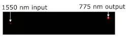
They used their approach to demonstrate the simplest example of a second-order nonlinear process: Second-harmonic generation, a.k.a. frequency doubling. To do it, the researchers fabricated a waveguide that converts continuous-wave telecom light to visible light (see figure below).
“When we first started the design process, we expected to need to resort to the usual phase matching tricks used for integrated photonics,” says Kéna-Cohen. “Very quickly, my Ph.D. student Pierre-Luc Thériault realized that because of the huge difference in refractive indices along different directions we could phase match the fundamental modes at both telecom and visible wavelengths by simply tuning the waveguide width.”
Another surprise is that “studying optical nonlinearities within these organic thin films has turned out to be a unique way to learn more about molecular orientation in general, and we have parallel work ongoing in that direction,” Kéna-Cohen adds.
One challenge along the way was that although the team’s films are quite robust thermally, they’re partly soluble within many solvents used for standard photolithography processes. “In our demonstration, we wanted to fabricate structures directly on top of the film,” says Kéna-Cohen. “So we developed a rather unique photolithography process that won’t degrade the organic layer in any way.”
Nonlinear materials for performance enhancements
What’s next? “Our best materials today have nonlinear properties similar to those of lithium niobate,” says Kéna-Cohen. “The main advantage is fabrication simplicity, but we think we can do much better. If we improve alignment during the deposition of layers, factors of >10x improvement are easily achievable in the very short term. This translates into factors of 100x improvement in efficiency for several devices.”
By using poled organic molecules, which is the traditional molecule-based approach, researchers can already achieve factors of >30x better than without poling. “For adoption, beyond fabrication simplicity, we need a big performance enhancement over the state of the art, and through our collaborations with chemists developing new materials we have a pathway to get there,” Kéna-Cohen says.
FURTHER READING
P.-L. Thériault et al., Sci. Adv., 12, eaeg3170 (2026); https://doi.org/10.1126/sciadv.aeg3170.
About the Author

Sally Cole Johnson
Editor in Chief
Sally Cole Johnson is Laser Focus World’s editor in chief, and she has more than 25 years’ experience as a science and technology journalist. She specializes in physics and semiconductors, and wrote for the American Institute of Physics for more than 15 years, and also covered theoretical physics and neuroscience for the Kavli Foundation, and complexity for the Santa Fe Institute. Johnson has also written extensively about military embedded systems, high-performance computing, software-defined networks, and infosec. She is a member of the National Association of Science Writers (since 2001).
When she isn’t writing about optics, photonics, or quantum advances, you can find her outside in northern NH in the garden with birds landing in her hand or heading for the mountains with her bike, skis, or crampons and ice axe.