Optical fiber brings ultralow signal loss to PICs

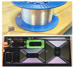
With “a simple but ambitious” motivation to bring optical fiber’s ultralow signal loss onto silicon chips, researchers in Professor Kerry Vahala’s lab at the California Institute of Technology (Caltech) are printing optical circuits made of optical fiber materials directly onto 8- and 12-inch silicon wafers (see video).
Using optical fiber as on-chip waveguides results in ultralow signal loss comparable to that of optical fiber at visible wavelengths.
“For decades, optical fiber has achieved extraordinarily low propagation loss using germanium-doped silica,” says postdoctoral scholar Hao-Jing Chen, who co-led the research with Kellan Colburn, a Ph.D. student.
But PICs have struggled to reach comparable performance with optical fiber—particularly at visible wavelengths, where scattering and material absorption become severe.
“Our approach brings the core material system of optical fiber (germanium-doped silica) into planar integrated photonics using a fully CMOS-foundry-compatible process,” Chen says.
Let’s unpack this
Part of the team’s work involves plasma-enhanced chemical vapor deposition (PECVD)—a vacuum process used to apply thin, high-quality solid films onto a substrate—of a 4-µm-thick germanium-silica (Ge-silica) layer on thermally grown oxide.
“Our process enables deep-UV stepper lithography for wafer-scale patterning and high-selectivity dry etching,” Chen says.
It also supports furnace reflow annealing to smooth sidewalls and suppress scattering. “This enables resonator intrinsic Q factors exceeding 180 million, from 458 nm to 1550 nm, with a peak Q of 463 million at 1064 nm,” Chen says, noting that this corresponds to 0.08 decibels per meter (dB/m) waveguide loss.
Their waveguides are laid out using a spiral geometry to extend their optical path length and transfer light efficiently between optical fibers and semiconductor lasers.
Notable findings
The team’s approach can produce 0.49 dB/m at 458 nm, which is a 13-dB improvement over previous visible integrated platforms. It can also produce 0.08 dB/m at 1064 nm.
“We’ve also seen 180-M intrinsic Q across the violet to telecom ranges, and a 10-dB improvement in anneal-free waveguide loss compared to previous records,” Chen says.
The team demonstrated three key device-level applications: Single-ring soliton microcombs with anomalous dispersion engineered in Ge-silica, stimulated Brillouin lasers enabled by acoustic confinement, and Hertz (Hz)-level narrow-linewidth visible lasers via self-injection locking.
“And in the visible spectrum, we achieved fundamental linewidths as low as 15 Hz at 632 nm, 12 Hz at 512 nm, and 90 Hz at 444 nm,” Chen says. “This represents a more than 20-dB improvement over state-of-the-art integrated visible lasers.”
Scaling hurdles
The team’s approach overcomes several longstanding challenges, including short-wavelength scattering loss. Chen explains that at visible wavelengths, Rayleigh scattering typically dominates. But his team’s furnace reflow process enables atomic-scale smoothness that suppresses the limitation.
They’ve also improved material absorption in the visible range.
“Many integrated materials, such as silicon nitride, show elevated absorption in the violet/blue regime,” Chen says. “Germanium-doped silica retains the low intrinsic material absorption known from fiber.”
Thermal budget constraints is another challenge their approach overcomes. “Our devices achieve ultrahigh Q, even without high-temperature annealing,” Chen says, “which enables compatibility with temperature-sensitive materials such as III-V, lithium niobate, and organic photonics.”
As far as key advantages of the team’s process, it operates in the broadband from 458 nm to 1550 nm, has record-low visible-band loss, and CMOS compatibility wafer-scale fabrication. It also touts dispersion engineering capabilities, acoustic confinement via germanium doping, and a large mode area for thermal noise suppression.
What’s next?
In the near term, the team will integrate rare earth dopants for on-chip amplifiers and lasers, as well as develop a visible-band frequency comb, and explore applications like precision metrology and quantum photonics.
“Long-term, our goal is to approach the material-limited loss of Ge-silica (~0.2 dB/km) on-chip,” Chen says. “This corresponds to microresonator Q factors exceeding 100 billion. This level of performance could fundamentally reshape technology such as portable optical clocks, chip-scale gyroscopes, integrated quantum photonic processors, low-noise microwave photonics, and high-power chip lasers.”
If the bigger picture for achieving fiber-like loss can be achieved at scale in CMOS foundries, the team envisions migration of traditionally fiber-based precision systems onto chips, visible integrated photonics with unprecedented coherence, and system-level integration for atomic, ion, and quantum platforms.
“In short,” Chen says, “this suggests the historical tradeoff between integration and performance may no longer be fundamental.”
FURTHER READING
H.-J. Chen et al., Nature, 649, 338–344 (2026); https://doi.org/10.1038/s41586-025-09889-w.
About the Author
 Justine Murphy
Justine Murphy
Multimedia Director, Digital Infrastructure
Justine Murphy is the multimedia director for Endeavor Business Media's Digital Infrastructure Group. She is a multiple award-winning writer and editor with more 20 years of experience in newspaper publishing as well as public relations, marketing, and communications. For nearly 10 years, she has covered all facets of the optics and photonics industry as an editor, writer, web news anchor, and podcast host for an internationally reaching magazine publishing company. Her work has earned accolades from the New England Press Association as well as the SIIA/Jesse H. Neal Awards. She received a B.A. from the Massachusetts College of Liberal Arts.