Laser wavelengths required for many of today’s most intriguing experiments, particularly within the visible range, are a challenge to source for tiny photonic integrated circuits (PICs). But U.S. National Institute of Standards and Technology (NIST) photonics researchers and colleagues at Octave Photonics are spearheading a solution to this wavelength access issue—and also addressing challenges to unite different photonic functions to support optical switching, routing, and filtering (see video).
One common approach today is to combine different photonics materials to attempt to enable these different functions and leverage strengths where they exist, but no single material can do it at all of the scales desired for fielding new applications.
“Our work was inspired by the lofty goal of achieving ‘any wavelength lasers,’ with direct compatibility to existing photonic technologies,” says Grant M. Brodnik, a physicist in NIST’s Quantum and Nonlinear Nanophotonics Group. “And we demonstrated other functionalities like frequency combs and supercontinuum generation, because the platform supports them directly. These capabilities play a key role in many important applications.”
Thank you, nonlinear optics
To reach the speed artificial intelligence (AI) and quantum applications demand, a shift from electrons to photons is critical—and so are chipscale “any wavelength” lasers.
A short explanation of the team’s new approach: It begins with a standard silicon wafer coated with silicon dioxide (glass) and lithium niobate, a nonlinear material that can alter the color of light entering it. Adding metal enables the lithium niobate to be electrically dialed-in for converting one color of light to others. Similar metal-lithium niobate interfaces can allow rapid on/off switching of light (think high-speed routing and data processing).
Depositing complex patterns of tantalum pentoxide, a.k.a. tantala, directly atop the other photonic circuitry allows versatile photonic platforms to operate in concert. Tantala is a strong nonlinear material and is well suited to visible wavelength operation. “Critically, it has appealing material properties (related to its fabrication) that make it amenable to direct integration with other photonic materials,” says Brodnik.
When the researchers patterned the materials atop of each other in a 3D stack, they ended up with a single chip that efficiently routes light between the layers. This chip combines tantala’s light manipulation abilities with lithium niobate’s controllability.
Nonlinear optics is the now “not-so-secret sauce” physics they leverage “to make entirely new colors of light out of the single color we put in,” explains Brodnik. “If you take a picture with a camera, you don’t expect the colors of the image to change when passing through a lens. But with nonlinear materials at high optical powers provided by lasers, it’s exactly what happens. It’s a key technique powering tabletop-scale lasers that make many custom colors today. We use these techniques—but with photonic circuitry within devices smaller than the size of a grain of rice.”
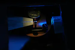
The coolest aspect of this work for Brodnik is seeing “new, often dazzling colors of light pop out of our devices from converting the input light (which is invisible to our eyes),” he says. “In the lab, with a chip sitting on a test stage, we slowly dial in the operation parameters and, boom, vibrant blue-green starts glowing across the chip. On the next device, we make it blue-violet. It feels a bit like magic.”
Their work “lays the foundation and demonstrates the potential of the platform,” says Brodnik. “We’ll certainly be working to optimize the performance of existing designs, but the platform unlocks new functionality and design knobs we’re excited to explore.”
Many applications that involve interfacing with atomic transitions—think quantum sensing and computing—require light at wavelengths spanning the visible and near-infrared wavebands. “Applications that need to rapidly route and switch light on/off, like optical data processing and computing, can benefit from the platform as well by leveraging other physics functionalities the materials provide,” Brodnik says. “Consumer display tech is perhaps another application. There are many more—certainly ones we haven’t even thought up, which can now be considered and developed by the scientific community.”
The team has “a handful of exciting photonic architectures currently in design stages, which require a full host of capabilities our platform supports,” says Brodnik. “We’re also excited to collaborate with colleagues and other researchers who’ve been bringing us new ideas and applications we perhaps haven’t considered or require shared expertise to pursue. Exciting times.”
FURTHER READING
G. M. Brodnik et al., Nature, 652, 899–905 (2026); https://doi.org/10.1038/s41586-026-10379-w.
About the Author

Sally Cole Johnson
Editor in Chief
Sally Cole Johnson is Laser Focus World’s editor in chief, and she has more than 25 years’ experience as a science and technology journalist. She specializes in physics and semiconductors, and wrote for the American Institute of Physics for more than 15 years, and also covered theoretical physics and neuroscience for the Kavli Foundation, and complexity for the Santa Fe Institute. Johnson has also written extensively about military embedded systems, high-performance computing, software-defined networks, and infosec. She is a member of the National Association of Science Writers (since 2001).
When she isn’t writing about optics, photonics, or quantum advances, you can find her outside in northern NH in the garden with birds landing in her hand or heading for the mountains with her bike, skis, or crampons and ice axe.