Disordered ‘mosaic’ metasurface enables multiple simultaneous optical functions
In an intriguing advance for metasurfaces, researchers at Monash University’s School of Physics and Astronomy in Australia came up with a disordered mosaic design approach—nanostructured materials that perform multiple simultaneous optical functions within a single device (see video).
The idea of a mosaic-style design for metasurfaces came to Haoran Ren, an Australian Research Council Discovery Early Career Research Award Fellow, who leads Monash’s NanoMeta Group, in a completely unexpected way.
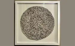
“In 2024, while attending the International Conference on Orbital Angular Momentum in South Africa’s Kruger National Park, I noticed an artwork on my hotel room wall,” Ren says. “The image immediately caught my attention with its clusters of colorful dots arranged in what looked like a completely random pattern. Their colors separated them into distinct groups—even though the overall layout was disordered.”
This made him wonder whether it was possible to do something similar for metasurface designs. “What if the metapixels responsible for a particular optical function were placed in a random distribution across the aperture? Multiple such sets could then coexist within the same device, each one selected independently by wavelength and polarization,” Ren says. “If we engineered strong optical selectivity, each function could be isolated without crosstalk. It felt like a powerful way to create a ‘knob’ to access independent photonic functions within a single metasurface.”
He phoned a friend, Changxu Liu, a disordered photonics expert at the University of Exeter, who immediately saw its potential. “Together, we developed a careful plan to test whether randomly arranged metapixels could still perform their intended functions, and to determine the limits of how much disorder the system could tolerate. It led us to a systematic set of simulations and, eventually, a full study,” says Ren.
Metasurfaces with multiple optical functions
Ren’s group at Monash includes Chi Li, a Research Fellow, who specializes in nanophotonics, metasurfaces, and two-dimensional materials, and they translated the visual idea into a physical design framework for metasurfaces—planar arrays of nanoscale structures that control light at subwavelength resolution.
“In a conventional metasurface, the entire aperture is used to implement a single function—such as a lens,” says Li. “We show this isn’t strictly necessary, because a given optical function can be achieved using only a randomly distributed subset of pixels. It allows us to assign different groups of metapixels—each corresponding to a distinct function—and distribute them across the surface in a disordered mosaic pattern. The key requirement is that each group can be selectively addressed, which we achieve by designing the nanostructures to respond to specific wavelengths or polarization states.”
As far as materials, the group uses silicon-based dielectric nanostructures for low optical loss, strong resonant behavior, and compatibility with standard semiconductor fabrication. “In this way, the mosaic concept becomes a practical strategy: Combining disordered spatial sampling with optical selectivity to integrate multiple independent functions within a single metasurface,” says Li.
Proof of concept: An optical metalens
The group’s device is a flat metalens and it focuses by encoding a phase profile using nanoscale structures. “A long-standing challenge within this field is chromatic dispersion—different wavelengths naturally focus at different distances and correcting this typically requires complex dispersion engineering, especially for large-aperture metalenses to be used in practice,” says Li.
Their approach takes a different route. Instead of forcing a single structure to work across all wavelengths, “we assign independent lens functions to different wavelength channels,” Li explains. “Each lens is implemented by a subset of metapixels, and these subsets are randomly distributed across the same aperture. As a result, each wavelength ‘sees’ its own lens, and chromatic aberration is removed without needing any dispersion balancing.”
It significantly reduces design complexity and, importantly, doesn’t compromise lens performance, because each channel operates as an optimized single-wavelength lens.
For polarization and structured light, “we apply the same principle of channel separation,” Li says. “Different metapixel groups selectively respond to different polarization bases and map them into distinct spatial outputs. This enables single-shot measurement of the full polarization state, even when it’s not spatially homogeneous but varies across the beam.”
The benefit is complex light fields—such as vector beams or topological structures—can be analyzed without scanning or multiple optical components to enable more compact, faster, and higher-resolution polarimetric imaging.
Performance gains
One of the most thrilling moment of this study for Ren was “when we realized just how well a disordered metasurface can perform,” he says. “Even when we placed the pixels in a completely random pattern, the function was preserved—not just with 10% of the pixels but even with 1% or less. The key was that this redundancy only works when the pixels are arranged with disorder.”
It was “remarkable because it meant all ‘unused’ pixels within the aperture could be reassigned to other functions, as long as we designed strong optical selectivity so each set could be individually addressed,” Ren says. “In other words: Disorder opened the door to packing multiple independent optical functions into the same metasurfaces without crosstalk.”
Controlled disorder challenges
The group faced challenges demonstrating that disorder can be used in a controlled and reliable way. “In optics, disorder is usually associated with performance degradation, so we needed to carefully verify—both numerically and experimentally—that the desired functions are preserved even when the metapixels are randomly distributed,” says Li.
Another challenge was achieving sufficiently strong optical selectivity. “Since multiple functions coexist within the same physical area, it’s essential that each set of metapixels responds only to its intended channel—whether it’s a specific wavelength or polarization,” Li points out.
After numerical verifications, fabrication posed practical challenges. “The device contains a large number of nanoscale features distributed over a millimeter-scale area, and maintaining uniform performance across the entire sample requires precise nanofabrication and process control,” says Li.
Simulations help push boundaries of disorder
Simulations played a central role in the group’s work to help figure out how far they could push the concept of disorder. “We systematically reduced the active area for a given function and compared ordered vs. disordered layouts,” says Li. “The result was quite striking: Ordered sampling degrades rapidly, while disordered sampling maintains near diffraction-limited performance even at very low area fractions.”
Another important aspect was identifying the minimum functional metapixel size. “We used simulations, and later experiments, to determine how small a metapixel can be while supporting the required optical response,” Li says. “This is critical because it defines the fundamental building block that makes large-scale multifunctional integration possible.”
The researchers also simulated multichannel devices—across wavelength and polarization—to confirm crosstalk remains low with sufficient selectivity.
Overall, these studies “not only validated the concept but established practical design rules for implementing disorder in metasurfaces,” says Li.
Wide range of photonics applications ahead
Optical systems underpin imaging, displays, communications, energy, and quantum technologies, and continued miniaturization is essential to drive innovation and reduce costs.
“Our disordered mosaic metasurface platform provides a versatile foundation for integrating multiple photonic functions into a single diffractive optical element, and it marks a significant step toward compact, high-density, multifunctional optical devices,” says Ren.
The group’s approach can support a wide range of photonic applications—such as combining polarization- or wavelength-specific functions within a shared aperture for advanced imaging, optical data multiplexing and communications, and even quantum key distribution. By enabling multiple independent functions to coexist without crosstalk, their platform opens new possibilities for highly integrated photonic systems.
“Another major advantage of our general design approach based on disordered mosaics is that it doesn’t introduce any additional computational complexity,” says Ren. “It allows multiple functions to be combined easily, without the heavy optimization normally required for multifunctional metasurfaces.”
Right now, the group is “identifying one or two ‘killer applications,’ where having several independent functions within a single metasurface truly solves a real-world problem,” Ren adds. “Once these use cases are clearly defined, we plan to build a business case for a startup and begin translating the technology into prototype devices. If everything progresses as expected, this could happen within the next two to three years.”
FURTHER READING
C. Li et al., Nat. Commun. (2026); https://doi.org/10.1038/s41467-026-71774-5.
About the Author

Sally Cole Johnson
Editor in Chief
Sally Cole Johnson is Laser Focus World’s editor in chief, and she has more than 25 years’ experience as a science and technology journalist. She specializes in physics and semiconductors, and wrote for the American Institute of Physics for more than 15 years, and also covered theoretical physics and neuroscience for the Kavli Foundation, and complexity for the Santa Fe Institute. Johnson has also written extensively about military embedded systems, high-performance computing, software-defined networks, and infosec. She is a member of the National Association of Science Writers (since 2001).
When she isn’t writing about optics, photonics, or quantum advances, you can find her outside in northern NH in the garden with birds landing in her hand or heading for the mountains with her bike, skis, or crampons and ice axe.