NIST scientists create PIC packaging that survives extreme temperatures
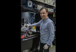
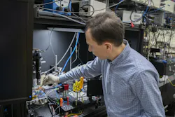
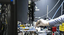
A multidisciplinary group of scientists led by Nikolai N. Klimov, Ph.D., principal investigator and project leader of the U.S. National Institute of Standards and Technology’s (NIST) Photonic Thermometry Program, created a new approach to couple optical fibers to a photonic integrated circuit (PIC) across an extraordinarily wide temperature range—from deep cryogenic conditions to very high temperatures (see video).
The inspiration behind their work was “both scientific and strategic,” says Klimov, whose team is working on developing an integrated photonics-based chipscale temperature standard, the Standard Photonic Thermometer (SPoT). It may eventually surpass and replace the world’s best resistance thermometers, the Standard Platinum Resistance Thermometers (SPRTs). “If we want a photonic thermometer capable of redefining temperature metrology, we first need to invent a packaging approach that can survive environments where no photonic package has ever been expected to operate.”
SPRTs set the benchmark for precision for decades, but are fragile, expensive, and limited to controlled laboratory environments. “If photonic thermometry is going to become the next-generation standard, it must be deployable as well as accurate,” Klimov says. “This is where packaging becomes mission critical. And this challenge—to create a robust, adhesive-free, alignment-stable fiber-to-chip interface for extreme environments—became the foundation of our work.”
Paradigm shift for photonic chip-fiber packaging
Most photonic packages rely on epoxies or polymers to hold fibers in place, but these materials simply can’t survive extreme temperature ranges—and tend to either soften, crack, outgas, or drift.
So Klimov and his team set out to create a photonic packaging method compatible with a wide range of harsh environments. “We also wanted it to be flexible enough to work with various photonic materials—such as silicon, silicon nitride, lithium niobate,” he says. “And it has to work with both edge optical coupling (array of fibers bonded to the facet of individual PIC die) and wafer-level packaging (array of fibers bonded to on-wafer surface grating coupler input/output ports).”
By using a silicate network hydroxide catalysis bonding (HCB) in lieu of traditional organic polymers, they’ve pulled off a paradigm shift in photonic chip-fiber packaging.
“During the HCB process, we form a very thin but extremely strong silicate network bonding layer between two joining oxide-terminated interfaces,” Klimov explains. “This method was originally developed during the 1980s at Stanford University. It was first used for the NASA satellite mission Gravity Probe B, and then a ground-based gravitational wave detector GEO600, and later for other astronomical applications. To our knowledge, there has never been a demonstration of HCB for PIC packaging with submicrometer alignment tolerances before.”
Monte Carlo simulations
While Klimov and colleagues didn’t run mechanical or thermal simulations of the HBC itself, they did perform an interesting set of Monte Carlo simulations that were “essential for understanding how much ionizing radiation the ultrathin HCB layer actually receives during extreme-environment testing,” he says.
After exposing a packaged photonic chip to a cumulative 1.1 megagray (MGy) of ionizing radiation—a typical chest x-ray is ~0.1 milligray—and confirming the assembly survived, the scientists wanted to know how much of the dose reached the merely 40- to 200-nm-thick HCB bonding layer.
Because the HCB layer is so thin and buried inside the assembly, “we did Monte Carlo modeling of the entire fiber-coupled chip package that was exposed to radiation,” Klimov says. “Our modeling showed the HCB layer received approximately 1.3 MGy, which is slightly higher than the external dose, due to the creation of secondary electrons within the silicon substrate layer of the PIC. And the HCB laser, only tens of nanometers thick, remained intact so we can couple light to the PIC.”
Coolest aspect of this work? “Our photonic chip packaging methodology can enable reliable PIC deployment to very harsh environments—from strong ionizing radiation to deep cryogenic or high temperatures to high- and extreme-high vacuum,” says Klimov. “Our fiber-coupled PIC is so rugged it survived—without any signs of bond degradation or loss of light coupling efficiency—a repeated rapid series of being dunked into liquid nitrogen.”
This packaging shows “clear potential for environments we haven’t even tested yet like high humidity and harsh chemical exposures,” Klimov says. “The structure of the hydroxide-catalysis bond (HCB) interface strongly suggests that the method could be extended to these conditions as well.”
Speed up cure time, scale up packaging process
While the group demonstrated their packaging approach can survive extreme temperatures, ultrahigh vacuum, and even a mega Gray of ionizing radiation, several challenges must be overcome before it becomes a fully deployable field-ready technology.
They still need to “characterize how it behaves over long-duration cycling: repeated temperature cycling from cryogenic to high-temperature transitions; months-long exposure to a vacuum; and extended radiation environments for space missions,” says Klimov. “Understanding long-term drift and stability is essential for a true metrology-grade standard.”
Speeding up the curing time is another challenge. “Right now, we cure the bond for one week, but we believe it can be shortened to a day or a few hours. We need to do more rigorous (extended) tests within harsh environments like humidity and chemical exposure,” Klimov says. “Once we reduce the curing time, we need to figure out how to scale up the packaging process to achieve high-volume production. We could test packaging reproducibility across multiple devices—with a timeline of 1 to 2 years.”
The structure of the HCB interface “suggests compatibility with high humidity environments and chemically harsh environments,” says Klimov. “We haven’t verified it experimentally yet, but demonstrating robustness within these conditions will open doors to industrial and environmental sensing applications.”
Target: Deployable systems
The core technology of the adhesive-free, extreme-environment photonic packaging “has been proven in the lab,” says Klimov. “This gives us a strong foundation to move from proof of concept toward deployable systems.”
Once reliability and manufacturability are established, the group’s long-term goals are to focus on testing deployments in space missions, nuclear facilities, cryogenic quantum systems, and harsh industrial environments. “These early adopters are the environments in which the advantages of thermometry, and the related need for robust photonic packaging, are the most dramatic,” Klimov says.
Klimov believes his group’s work “will impact the photonics community by expanding the reach of photonics into new extreme environment applications, including temperature sensing for nuclear power plants and space,” he says. “Our method could also support emerging applications such as photonic quantum computing, quantum communications, quantum optomechanics experiments, and single-photon emission and detection that requires reliable photonic fiber-to-chip packaging at cryogenic temperatures.”
FURTHER READING
S. M. Robinson et al., Photon. Res., 14, 1505–1516 (2026); https://doi.org/10.1364/prj.565679.
Related Webinar
About the Author

Sally Cole Johnson
Editor in Chief
Sally Cole Johnson is Laser Focus World’s editor in chief, and she has more than 25 years’ experience as a science and technology journalist. She specializes in physics and semiconductors, and wrote for the American Institute of Physics for more than 15 years, and also covered theoretical physics and neuroscience for the Kavli Foundation, and complexity for the Santa Fe Institute. Johnson has also written extensively about military embedded systems, high-performance computing, software-defined networks, and infosec.
When she isn’t writing about optics, photonics, or quantum advances, you can find her outside in northern NH in the garden with birds landing in her hand or heading for the mountains with her bike, skis, or crampons and ice axe.