AI drives optical interconnect adoption for scalable GPU communication
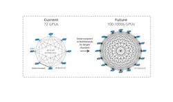
At the heart of modern artificial intelligence (AI) is matrix multiplication. Large neural networks can distribute arithmetic across many processing elements at once, which makes parallel computing the obvious way to increase performance. This approach works well up to a point—but once models grow past roughly ten billion parameters, scaling can no longer be handled inside a small local compute domain. The workload must be distributed across many graphics processing units (GPUs), spanning the range of scales from internal boards and servers to integrated racks and, increasingly, multi-building regional fabrics.
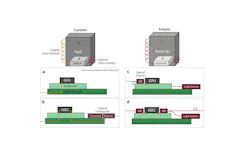
In practice, GPUs need to behave as one much larger processor. This means a constant exchange of gradients, parameters, activations, and synchronization traffic across the cluster. At this scale, network performance becomes inseparable from compute performance: If data can’t move quickly enough, the accelerators wait. It’s where the industry runs into what many call the “copper wall,” which creates a bottleneck at the latency-sensitive level of the hierarchy and obstructs high-speed links required to bridge GPUs within a scale-up cluster (see Fig. 1).
It’s necessary to point out up front that copper is not obsolete. Over short distances, electrical interconnects remain mature, cost-effective, and highly practical. But for 200-Gbit/s-per-lane signaling, the tradeoffs become much harsher. The reach of direct-attach copper shrinks to 1 to 2 meters at 200 Gbit/s per lane, while extending reach further requires retimers and adds both power requirements and cost. As AI scale-up clusters become larger and denser, copper simply can’t keep up. The next step for the industry is to switch to optical communication to enable higher bandwidth, higher speed, higher radix, and lower energy consumption.
Optics move inward
Optical communication is already established for scale-out networking, particularly rack-to-rack and row-to-row links. The trend now is the architectural question of where the electrical-to-optical boundary should sit for future AI systems. The Open Compute Project’s Short Reach Optical Interconnect effort, for example, is focused on improving processor-to-processor and processor-to-memory bandwidth by defining the requirements and metrics for optical interconnects (see Fig. 2).
In a conventional pluggable-optics design, the electrical signal must travel across the board before it reaches the transceiver and is converted to light. At the highest data rates, these electrical paths become increasingly painful in terms of loss, equalization, power, and layout complexity. Co-packaged optics (CPO) shortens this path by placing the optical engine directly adjacent to the chip package to reduce the length of high-speed copper traces and create a more credible route to higher bandwidth density and lower energy per bit. And the traditional transceiver is instead split into an optical engine near the chip, an external laser source, and the fiber interconnect.
The industry is increasingly moving toward external-laser architectures because lasers are thermally sensitive and easier to manage when separated from the hottest parts of the package. Both NVIDIA and Broadcom announced major developments in CPO technology in 2025, and volume roll-out is expected between 2028 and 2030.
CPO: Exceptional appeal, but far from easy
CPO is fundamentally a heterogeneous integration problem. Different materials systems, device types, and manufacturing processes must all come together in a compact, high-performance package. Multiple laser strategies are under consideration, as well as multiple modulator approaches, and different ways to partition functionality between the optical engine, light source, and host application-specific integrated circuit (ASIC). Each design choice affects footprint, insertion loss, thermal sensitivity, manufacturability, cost, and long-term reliability. The challenge isn’t merely to build a fast optical link, but to build one that survives packaging, qualification, volume manufacturing, and field deployment. The industry is reacting to these challenges as reflected by the flurry of multisource agreements announced surrounding the 2026 Optical Fiber Conference (OFC), such as the Optical Compute Interconnect Multisource Agreement or Open Co-Packaging Multisource Agreement industry consortia.
Thermal management is one of the most difficult parts of the problem. GPUs and switch ASICs already operate within extremely demanding thermal environments. Bringing optics closer to these devices raises immediate concerns around laser lifetime, modulator behavior, packaging interfaces, and overall system stability. One reason external-laser architectures are gaining traction is because they allow designers to move one of the most temperature-sensitive elements away from the hottest region. But this choice introduces its own packaging and systems tradeoffs, such as alignment, routing, serviceability, and total system complexity.
Manufacturing adds another layer of difficulty. Consider the number of fibers exiting the optical engine. In principle, the more individual fibers the more parallel the AI clusters—and flatter network topologies. In practice, however, fiber attach is one of the most difficult and expensive parts of optical assembly, especially when active alignment is required. Every additional fiber can affect yield and cost. It means the winning solution will not necessarily be the one with the most elegant device physics but rather the one that best balances bandwidth, assembly complexity, thermals, and manufacturability.
All of these aspects combined clarify the broader arc. AI first made parallel computing essential. Then, it made distributed computing unavoidable. Now, it is forcing a rethinking of interconnect architectures. Optical links have already become standard in longer-reach data center networking. The next step is much closer to the compute package itself, where copper increasingly struggles to satisfy the combined demands of bandwidth, reach, and energy efficiency. CPO is emerging as one of the leading answers to this problem—not because it is easy, but because the alternative is becoming harder to scale.
FURTHER READING
- TDK Ventures, “Why We Invested in Mixx Technologies” (2025)
- NVIDIA, “NVIDIA Announces Spectrum-X Photonics, Co-Packaged Optics Networking Switches to Scale AI Factories to Millions of GPUs” (Mar. 18, 2025)
- Broadcom, “Broadcom Announces Tomahawk 6 – Davisson, the Industry’s First 102.4-Tbps Ethernet Switch with Co-Packaged Optics” (Oct. 8, 2025)
- Open Compute Project, “Short Reach Optical Interconnect”
- OCI MSA, “Optical Computer Interconnect Multi Source Agreement”
- OpenCPX MSA, “OpenCPX MSA – Open Compute Project Multi Source Agreement”
About the Author
Tina Tosukhowong
Tina Tosukhowong is the investment director for TDK Ventures (Boston, MA), where she leads the cleantech and advanced materials investment areas. She holds a Ph.D. in chemical engineering and a certificate in management of technology from Georgia Institute of Technology. She is also a graduate of Harvard Business School’s Private Equity and Venture Capital program.
Dante Zakhidov
Dante Zakhidov is an investment analyst for TDK Ventures (Boston, MA), and focuses on advanced materials for semiconductor, photonic, quantum, and energy technologies. He holds a bachelor’s degree in chemistry from Rice University and a doctorate in materials science and engineering from Stanford University.