Nanometer precision at scale: Active-alignment fiber arrays unlock next-gen photonics
Photonic quantum computing is advancing rapidly—but scaling hardware platforms requires more than qubit innovation. Fiber-to-chip connectivity, in particular, is emerging as an engineering constraint.
Photonic quantum computers rely on multichannel fiber arrays to couple light into photonic integrated circuits (PICs). Even nanometer-scale misalignment can introduce photon loss, degrade entanglement fidelity, and impact overall system performance. While conventional fiber arrays developed for datacom and telecom applications offer high throughput, they were not designed to meet the ultralow-loss requirements of quantum architectures. As the industry transitions from research prototypes to early commercial systems, packaging precision must evolve from a laboratory challenge to an industrial capability.
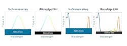
The precision advantage that active alignment delivers extends well beyond quantum systems. Any photonic application operating with tight optical loss budgets—whether for space communications, defense sensing, datacom, or telecom infrastructure—benefits directly from lower insertion loss and tighter channel-to-channel uniformity. For analog optical sensing applications, reduced coupling loss enables detection of weaker signals and more efficient use of the full laser bandwidth of, for example, a superluminescent light-emitting diode (SLED; depicted in the figure below on the right and left, respectively). Lower loss also means less laser drive power is required to meet a given optical budget: Lasers run cooler, generate less waste heat, and last longer. The result is a smaller thermal footprint, reduced cooling overhead, and improved product lifetime across the board.
Moving beyond passive alignment
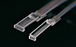
MicroAlign developed a micromanipulation platform to actively align individual fibers with nanometer-level precision. Traditional fiber arrays rely on passive placement into precision V-grooves, where mechanical tolerances accumulate across channels. Active alignment, by contrast, dynamically adjusts fiber position during assembly, correcting pitch deviations before permanent fixation. This approach enables multichannel arrays optimized for minimal insertion loss.
As performance targets tighten, optical-coupling losses below 0.5 dB are increasingly expected in quantum and other high-end photonic applications. Maintaining such loss levels consistently across production volumes requires not only precision, but also repeatable process control.
Scaling production for emerging demand
To support industrialization, MicroAlign secured a €2.5M ($2.8M) EIC Accelerator Grant, which includes an equity component, to accelerate automation of our fiber-array manufacturing. The funding supports scaling production throughput while maintaining consistent, high-quality output. This transition is critical as quantum computing companies begin planning larger-scale deployments. Fiber arrays are not marginal subsystems within photonic quantum computers. A single large-scale system can require thousands of arrays. As adoption accelerates, a reliable and scalable supply chain is strategically important.
Higher density and tighter pitch
Beyond scaling throughput, we’re also addressing density. During 2026, MicroAlign plans to introduce a new generation of ultrahigh-accuracy fiber arrays with channel pitches down to 127 µm. Reducing pitch enables more compact photonic packaging and supports higher I/O density on integrated chips. As photonic circuits incorporate increasing channel counts, dense fiber arrays become essential to maintain manageable footprints and routing complexity.
Active alignment offers advantages in such dense configurations, where small positional errors can significantly affect aggregate optical loss across multiple channels.
Beyond quantum applications
Although quantum computing is a primary driver, the need for ultralow-loss connectivity extends into many other advanced photonic domains—and the commercial opportunity in these markets may prove just as significant.
In optical switching and routing, microelectromechanical systems (MEMS) switches and wavelength-selective switches are core components of reconfigurable networks for datacenters and telecom backbones. These devices are highly sensitive to insertion loss: Every additional 0.1 dB of coupling inefficiency at the fiber-to-chip interface directly erodes system margin and may force the use of more costly optical amplification. Active-aligned arrays capable of consistently hitting sub-0.5 dB loss targets enable system designers to relax amplifier requirements, reduce power consumption, and extend reach without added infrastructure.
Defense and space photonics present an equally compelling case. Free-space optical communications terminals, LiDAR sensors, and satellite payloads all demand the highest possible coupling efficiency to operate reliably under constrained size, weight, and power (SWaP) budgets. For these environments, a fraction of a decibel saved at the fiber-chip interface can translate directly into a smaller, lighter, longer-range system. Performance uniformity across all channels—a hallmark of active-aligned arrays—is especially critical for multichannel sensor arrays in which channel-to-channel variation can degrade measurement accuracy.
By 2029, MicroAlign aims to support a significant share of photonic quantum computing systems worldwide with its ultrahigh-accuracy fiber arrays. Our roadmap also targets fast-growing non-quantum segments, including optical switching, coherent communications, sensing, and defense photonics—where the same precision manufacturing capabilities address well-established and urgent customer needs.
Precision packaging as a competitive differentiator
The industrialization of active alignment reflects a broader shift for photonics manufacturing. Fiber arrays are evolving from commoditized telecom components into precision-engineered subsystems central to system performance—across quantum computing, advanced sensing, optical communications, and defense photonics.
Emerging quantum and high-end photonics markets are redefining expectations: Nanometer-scale pitch accuracy, sub-0.5 dB coupling loss, high channel density, and scalable automation. Meeting all four simultaneously requires rethinking assembly methodologies.
As photonic quantum computing moves toward commercial deployment, the scalability of packaging technologies may prove as critical as advances in qubit architectures. And for the many high-performance photonic markets that don’t involve a single qubit, the same lesson applies. In an industry where every fraction of a decibel matters, precision packaging is no longer a detail—it’s a strategic advantage.
About the Author

Dario Lo Cascio
Dario Lo Cascio is the program manager for MicroAlign, a photonics technology company based in Eindhoven, The Netherlands.