Large triple-junction perovskite-perovskite-silicon tandem solar cell sets efficiency record
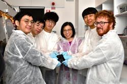
A team of researchers led by Professor Anita Ho-Baillie, the John Hooke Chair of Nanoscience at the University of Sydney in Australia, set a new solar technology record for the world’s largest triple-junction perovskite-perovskite-silicon tandem solar cell.
Their 16-cm2 triple-junction cell features a steady-state power conversion efficiency of 23.3% (independently certified), which is the highest reported for a large-area device of its kind. Her team also created a 1-cm2 cell with 27.06% efficiency, which established new thermal stability standards (see video).
The push for efficiency gains is driven by “larger headroom for power conversion efficiency—because the theoretical efficiency limit for a triple junction is ~51%, while for a double junction it’s around 45%,” says Ho-Baillie, who is also affiliated with the University of Sydney’s Net Zero Institute. “A single junction is 33% if the bandgap of the solar cell isn’t constrained, but only 30% for silicon.”
Multijunction tandem solar cells involve stacking solar cells with different bandgaps—with the highest on the sun-facing side—to allow each cell to convert sections of the solar spectrum to electrical energy more efficiently and to minimize sub-bandgap and thermalization losses.
“In a two-junction cell, for example, the top wide-bandgap junction converts higher photon energy to electrical energy and does it more efficiently than a narrower bandgap junction—which reduces thermalization loss,” explains Ho-Baillie. “The lower-energy photon passes through the top wide-bandgap junction and will be absorbed by the narrower bandgap bottom junction for electrical energy conversion. If the bottom junction wasn’t there, such lower-energy photons result in sub-bandgap nonabsorption loss.”
Optical designs
To illustrate the optical designs involved, the team’s top two perovskite junctions are electrically interconnected through gold nanoparticles. “We used optical modeling to simulate the effect of nanoparticle coverage on optical loss, and electrical modeling to simulate the ohmic contact made by the nanoparticle,” explains Ho-Baillie. “A balance is struck when a sufficient number of nanoparticles are present for minimum optical loss without compromising electrical performance.”
Ho-Baillie’s team also improved the stability and performance of the wide bandgap (1.91-eV) perovskite junction by “replacing rubidium with the less stable methylammonium in the perovskite and replacing piperazinium-dichloride (PDCI) with the less stable lithium fluoride as a surface passivating layer,” she says.
Ho-Baillie’s persistence in wanting to visualize the ultrathin gold really paid off. “There needs to be a critical amount of gold for clusters to form to first become a semicontinuous film,” she says. “More gold will enable a continuous film to grow. Below the ‘cluster’ critical amount, gold will be in the form of nanoparticles. What makes our findings interesting is that films—continuous or not continuous—aren’t needed to connect two junctions. Nanoparticles, although isolated, are sufficient for ohmic contact between the junctions for vertical carrier transport—while minimizing optical losses.”
What does this efficiency record mean for the field? “Our demonstration provides insights into important material properties for future efficiency improvements,” says Ho-Baillie. “Loss analysis also provides recommendations for future efficiency improvements—both for small- and large-area devices. Next up: A 30% triple junction, pushing toward 40%.”
The team’s work involved partners from China, Germany, and Slovenia, and received support from the Australian Renewable Energy Agency and the Australian Research Council.
FURTHER READING
J. Zheng et al., Nat. Nanotechnol. (2025); https://doi.org/10.1038/s41565-025-02015-x.
About the Author
Sally Cole Johnson
Editor in Chief
Sally Cole Johnson, Laser Focus World’s editor in chief, is a science and technology journalist who specializes in physics and semiconductors.

