Foundry to frontline: Key takeaways from AMF’s ‘Silicon Photonics Ecosystem Summit 2025’
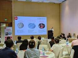
AMF’s recent event brought together industry leaders to discuss the ways silicon photonics (SiPh) is maturing from a promising technology into a foundational standard for the next-generation high-speed data infrastructure. The summit’s central theme was SiPh at scale, and it provided a strategic roadmap to advance SiPh technology to meet rapidly accelerating production and unprecedented performance demands. AMF, led by a management team including CTO Patrick Lo Guo Qiang, organized the summit to showcase the collaborative ecosystem driving innovation.
AMF keynote: Scaling a $37B opportunity
The summit began with an introduction from AMF leadership and emphasized the seismic shift occurring within the market. The sheer growth of artificial intelligence (AI) workloads is driving demand for high-speed transceivers and rapidly expanding the total addressable market (TAM) for SiPh capabilities, including LiDAR and sensing. The overall optical components market is projected to reach $37B by 2029, growing at a 19% CAGR.
As a dedicated SiPh foundry, AMF is strategically positioned to capture this growth, with anticipated revenue growth of 82% from FY24 to FY25, driven by 400Gbe and 800Gbe. AMF offers core technology optimized for data centers, telecom, and sensing, with services ranging from high-volume manufacturing to multi-project wafer (MPW) shuttles—including the launch of new high-performance (HP) MPW runs, which started in September 2025.
Session 1: The AI computing tsunami and SiPh dominance
Carol Cao, senior analyst at LightCounting, delivered the opening guest presentation and described how AI computing is redefining network demands.
Unprecedented requirements. AI computing clusters require approximately 3x the quantity of optical components compared to general computing. Furthermore, AI requires dramatically higher bandwidth (>2x) and critically, low power consumption and ultralow latency.
Scale-up and scale-out. The expansion of AI clusters is astonishing, with typical large clusters jumping from 4,000 graphics processing units (GPUs) in 2022 to 100,000 in 2024. Projections for 2025 reach a colossal one million GPUs. This growth is driving new market opportunities for SiPh, especially for scale-up scenarios that require nanosecond latency.1
A technology shift to copackaged optics (CPO) and linear pluggable optics (LPO). To handle these demands, the industry is accelerating the adoption of CPO and LPO). CPO, which offers higher bandwidth density and lower latency than traditional pluggable modules, is rapidly maturing and is demonstrated by products like Broadcom’s Tomahawk 6 102.4-Tbps switch.
SiPh is key. Ms. Cao noted that SiPh is overcoming early debates about its future. Due to the rapid growth in 400G and 800G demand in 2024, the penetration rate of SiPh modules surged. SiPh offers easier capacity increases, stable performance, and a clear, reducible cost advantage. The conclusion of the market analysis is clear: SiPh will be the dominant technology for LPO and CPO.
Session 2: Accelerating design for complex hybrid systems
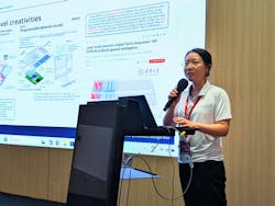
Ruping Cao, president of Luceda Photonics, discussed the sophisticated design solutions required to bring these complex SiPh systems to life.
PIC trends. Current photonic integrated circuits (PICs) are defined by three major trends: System-level creativity, the integration of different material platforms (hybrid integration, wafer/die bonding, printing), and the closer integration of photonics with computing functions.
The PDK-driven workflow. To manage this complexity and accelerate time-to-market (TTM), Dr. Cao highlighted the necessity of a reliable, scalable design flow. Luceda’s IPKISS framework uses a code-driven flow and parametric cells (PCell) to link the foundry’s process design kits (PDKs) directly into the design process. This helps PIC designers achieve the same capabilities and rigorous verification enjoyed by electronic IC designers.
Ensuring yield and reliability. The workflow supports advanced circuit analysis methodologies, such as corner analysis and layout-aware variability analysis, used to optimize designs for yield and reliability. Crucially, the system must support multiple PDKs, Assembly Design Kits (ADKs), and testing design kits (TDKs) to handle the varied and closer integration formats required by next-generation hybrid systems. Luceda demonstrated working with the AMF PDK platform.
Session 3: Mastering heterogeneous light source integration
The final presentation, delivered by Jian Yin, manager of the Edge-Emitting Laser Department at Advanced Micro Semiconductors (AMSFAB), addressed the core manufacturing challenge: Integrating high-performance light sources onto SiPh chips.
AI drives the need for Integration. The SiPh market through 2028 will mainly be driven by an optical module demand from AI data centers. Light source integration is critical, and due to cost demands and technical maturity, heterogeneous integration is the primary development approach.
Two paths to integration. Dr. Xu’s team explored two key methods for merging III-V materials (for light emission) with silicon PICs:
- Microtransfer printing (MTP). This technique transfers pre-processed III-V laser chips onto a silicon PIC wafer. Key advantages include the reuse of the III-V substrate (lowers cost) and the potential for wafer-level testing (reduces chip test time from 200 hours to 60 hours on a 4-inch wafer).
- Direct bonding (heterogeneous fabrication). This involves bonding the III-V epitaxial wafer directly to the silicon wafer before processing, and enables easier evanescent wave coupling and the highest integration density.
AMSFAB’s capability. AMSFAB, a compound semiconductor foundry platform, is supporting the complex fabrication needed for both methods, offering capabilities for critical processes like creating etched facets and tether structures for MTP, and implementing the required flip-chip epi design for direct bonding.
The ecosystem powering SiPh
Our summit confirmed that SiPh is the indispensable foundation to meet the explosive demands of AI computing. This market transition is enabled by the close cooperation demonstrated by the ecosystem: market analysis identifying the need (LightCounting), advanced design frameworks ensuring manufacturability (Luceda), and specialized foundry capabilities (AMF and AMSFAB) mastering the challenges of heterogeneous integration.
As the dedicated host and a pure-play silicon photonics foundry, AMF demonstrated its central role in driving innovation by bringing together the critical voices and technologies required to move silicon photonics from niche application to silicon photonics at scale.
REFERENCE
About the Author
Pratirupa Sarkar
Pratirupa Sarkar is a corporate marketing and analytics engineer for Advanced Micro Foundry (AMF), which is a pure-play silicon photonics foundry based in Singapore.


