MIT creates evanescent coupler to copackage electronics and photonics
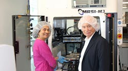
In August 2024, Laser Focus World introduced you to the FUTUR-IC work led by Massachusetts Institute of Technology’s (MIT) Anuradha Murthy Agarwal and Lionel C. Kimerling to enhance microchip performance by integrating electronics with photonics—in a scalable and environmentally sustainable way.
Related Article
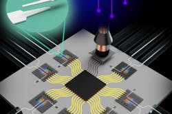
One year later, the group has created an evanescent coupler to copackage photonics and electronics. Integrating photonics with electronics within the same package “is the transistor for the 21st century,” says Kimerling, a professor of materials science and engineering at MIT, as well as director of MIT’s Microphotonics Center.
Significantly, the group’s evanescent coupler enables manufacturing on existing electronics foundries’ equipment with a less expensive passive alignment process.
It also handles the optical fiber baggage that comes along with copackaging electronics and photonics into a single package: The optical fiber (core diameter of 10 µm) that connects them must be precisely aligned with the photonic chips (cross-sectional dimensions of merely 0.2 µm × 0.5 µm) or the light will disperse. Today, this means each connection must be actively tested with a laser to ensure light passes through.
Since the number of fibers necessary for greater data communication is increasing exponentially, this active alignment process “won’t cut it for scaling forward,” points out Drew Weninger, who worked with Kimerling and recently completed his Ph.D. at MIT.
The group’s evanescent coupler provides “wiggle room” connecting the fibers within an electronic-photonic package. While conventional couplers have a single coupling point, which makes alignment tolerances tight, this one features “a much larger interaction length that increases the alignment tolerance,” says Agarwal, a principal research scientist at MIT’s Materials Research Lab.
Why is this a big deal? It means robots can passively assemble the resulting copackaged integrated circuits (ICs) to let more light to pass through—without active laser alignment.
It can also transmit light vertically between multiple layers of chips, which is difficult to pull off because it involves pulling light out of a horizontal plane. For electronics, this is simple because “electrons can easily flow out of plane,” says Weninger. “Light never wants to take right angles,” but this is where the evanescent coupler comes in.
The group’s packaging/interconnect design is “reliable, has a larger alignment tolerance, doesn’t lose much light, and doesn’t waste much space,” says Luigi Ranno, another group member who worked on the coupler and recently completed his Ph.D. at MIT.
Congrats to the group!
FURTHER READING
D. Weninger, S. Serna, L. Ranno, L. Kimerling, and A. Agarwal, Adv. Eng. Mater., 27, 4, 2570012 (Feb. 2025); https://doi.org/10.1002/adem.202570012.
About the Author
Sally Cole Johnson
Editor in Chief
Sally Cole Johnson, Laser Focus World’s editor in chief, is a science and technology journalist who specializes in physics and semiconductors.


