Small-scale optics: Trends, engineering challenges, and strategic solutions
As industries such as consumer electronics, healthcare, and telecommunications increasingly embrace miniaturized optical technologies, research and development (R&D) managers face mounting pressure to drive innovation while optimizing efficiency, cost, and time-to-market. Small-scale optics, which power advancements for applications such as augmented reality (AR) glasses, three-dimensional (3D) sensing, and high-speed data communications, are at the heart of this transformation. But unlocking the full potential of these advancements comes with significant engineering and operational challenges.
Trends driving small-scale optics
One of the most prominent trends in optics is the drive toward miniaturization. Consumer demand for smaller, lighter, and more powerful devices is pushing engineers to design compact, high-performance optical systems. The challenge lies in ensuring performance is not compromised as form factors shrink. Micro-optics, waveguides, and metasurfaces are increasingly seen as critical components for system design, especially for applications such as augmented reality and virtual reality (AR/VR), where size, weight, and power (SWaP) may be more important considerations than component complexity. Photonic integrated circuits (PICs) are another solution for device miniaturization (think LiDAR systems for autonomous vehicles) gaining traction within the market.
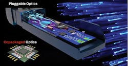
The move from pluggable to near-package (NPO) and copackaged (CPO) optics marks another transformative trend to enable high-speed, low-power data transmission by integrating multiple components on a single chip. NPO and CPO offer greater functionality in smaller footprints, helping to push the boundaries of what’s possible for modern data centers. These innovations are fueling telecommunications and high-performance computing advances, by enabling engineers to adopt cost-effective, scalable design approaches.
Metasurfaces, a.k.a. “flat optics,” are also shifting traditional optical design paradigms. These nanostructured, ultrathin materials offer unprecedented control over light, which allows engineers to rethink manufacturing processes while balancing cost and performance. Unlike conventional lenses, metasurfaces offer a highly customizable approach to manipulating light—unlocking new possibilities for imaging, sensing, and optical computing.
Artificial intelligence (AI) is also poised to revolutionize optical system design and development by allowing engineers to more efficiently explore new and innovative system architectures and to more effectively optimize these architectures for specific system requirements. These advances will enable faster, more efficient development processes to meet performance and manufacturability criteria.
Industry challenges
Despite the promise of small-scale optics, engineers face numerous challenges. Increasing design complexity is one of the most pressing concerns. As optical components shrink, ensuring accurate system behavior and minimizing losses becomes more difficult. Engineers must accurately model interactions from the nanoscale to the system level, which requires them to use sophisticated tools to predict light propagation and optimize system performance across all scales.
Scaling these designs from prototype to mass production is another challenge. Manufacturability remains a critical consideration, because not all innovative optical designs are easily transferable to high-volume production. Engineers must also contend with the delicate balance between size reduction and performance to ensure metrics such as efficiency and image quality are maintained while mitigating issues like optomechanical stray light and thermal effects. Cost and time constraints further complicate the process. Prototyping and experimental testing at the nanoscale are both expensive and time-intensive, which increases the risk within the product development pipeline. The need for virtual validation tools for rapid design iteration is more pressing than ever to help engineers eliminate costly errors before committing to physical prototypes.
Simulation solution
To tackle these challenges, engineers must adopt an integrated approach that includes advanced multiscale, multiphysics simulation. A comprehensive understanding of how optical, thermal, and mechanical factors interact is essential to preempting design issues before they arise. Virtual prototyping allows for rapid iteration, which reduces the reliance on physical testing while ensuring that designs meet performance and manufacturability goals. Cost-effective virtual prototyping plays a crucial role minimizing development risks.
AI-powered optimization tools are also essential in this strategy. Automating the iterative design process enhances efficiency, enabling engineers to explore a broader design space and generate optimal solutions faster. These tools also improve manufacturability, ensuring that designs are not only high-performing but also suitable for mass production. Integrating cost-effective virtual prototyping with AI-powered optimization tools provides high-fidelity software modeling, allowing engineers to refine optical systems without the need for excessive physical prototypes, speeding up innovation cycles, and improving time-to-market.
Multiscale, multiphysics simulation tools help overcome challenges designing systems with small-scale optics. State-of-the-art modeling capabilities accelerate development cycles, reduce risk, and lower costs. Ansys Optics’ multiphysics simulation capabilities enable evaluation of optical systems under real-world conditions to account for electromagnetic, thermal, and mechanical factors. This holistic approach ensures optical systems perform optimally within the field while minimizing the risk of failure after deployment.
At the nanoscale, Ansys Lumerical provides tools for modeling photonic components—from waveguides to image sensors, light-emitting diodes (LEDs) to vertical-cavity surface-emitting lasers (VCSELs), diffraction gratings to metasurfaces, and much more. It also supports modeling of PICs at the device level, for robust co-simulation of electro-optic and electronic-photonic design automation (EPDA) workflows. As the field of quantum optics continues to evolve, it provides tools to model quantum effects with high precision—which is crucial for emerging technologies like quantum computing, secure communications, and ultra-efficient optical devices—to empower R&D teams to push the limits of optical innovation with confidence.
Within the realm of macroscale optical component design, where geometric optics (with occasional assistance from wave optics) is used to accurately characterize component performance, Ansys Zemax plays an important role. For applications ranging from cell phone cameras to CubeSat optical system development to wearable sensors to fiber-to-chip coupling units, OpticStudio helps engineers design, analyze, and optimize compact, high-precision optical systems. It provides a focus on the design for manufacture with a set of tools to evaluate the impact of manufacturing and assembly errors on system performance. And it seamlessly integrates with mechanical design workflows to ensure optical components fit within space-constrained environments while maintaining performance and manufacturability.
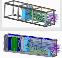
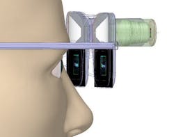
At the system level, Ansys Speos provides powerful simulation capabilities that support precise design visualization and validation of devices leveraging small-scale optics. Beyond providing tools for the design and optimization of high-precision lighting and illumination systems (such as automotive headlamps and cell phone displays), it allows small-scale optics such as waveguides and microlenses to be integrated into system-level models for applications ranging from AR/VR headsets to automotive head-up displays (HUDs) and more. This integration allows designers to evaluate the performance of photonic and optical components being used to construct their systems within the context of the full-scale 3D environment in which these components will be deployed. It also enables designers to account for human perception and visual acuity when evaluating system performance, which (for example) allows the designer to prototype the actual user experience for someone looking through a set of AR glasses.
Ansys Optics’ simulations provide seamless integration with existing R&D workflows to enable a cohesive process from design through simulation to manufacturing. This integration reduces iteration cycles, accelerates product innovation, and allows companies to bring cutting-edge optical technologies to market more efficiently.
Competitive advantage for R&D
The future of optics lies in the strategic use of advanced tools and technologies. To remain at the forefront of optical development, industry leaders must embrace digital prototyping, AI-driven optimization, and integrated simulation workflows. Ansys equips engineering teams with the capabilities to navigate the complexities of small-scale optics and stay ahead in an increasingly competitive market.
About the Author

Sanjay Gangadhara
Sanjay Gangadhara is the senior program director for Optics at Ansys Optics (Canonsburg, PA). In this role, he works closely with the leadership teams from product management and R&D to define the long-term product vision and business strategy for the Ansys Optics portfolio. As a part of this effort, Sanjay leads strategic partnership and business development activities within Ansys Optics and serves as a brand ambassador for the Optics portfolio. His background in general physics, electromagnetism, and optical systems diagnostics has served him well in his various roles throughout his career. Sanjay holds a Bachelor’s degree in Chemical Engineering & Nuclear Engineering from UC Berkeley and a Ph.D. in Nuclear Science & Engineering from MIT.