Co-packaging photonics and electronics poses challenges
We know optics is fantastic for communications via moving data, but how can we insert photonics into computing systems of various sizes from on-chip systems to large-scale computers? And what’s the best way to bring data movement into the optical domain to computing?
These are two of many questions Keren Bergman, a professor of electrical engineering, as well as scientific director of the Center for Integrated Science and Engineering at Columbia University, is currently exploring at the intersection of optics, photonics, and computing.
The drive to bring photonics into computing systems is motivated in large part by a Cambrian-like explosion of artificial intelligence (AI) applications in machine learning, because most data centers around the globe are running AI applications.
“We’ve made tremendous advances in optical communications during the past decade,” says Bergman. “In the past, we primarily used optical communications for long-haul fiber-optic systems. But recent advancements are enabling the integration of optics on chip—in the form of silicon photonics—and bringing the optical interface from the electronic plane to the optical plane all the way into the chip.”
And it presents opportunities: Can the optical interface be connected to the computer chip and memory chip to enable optical communications within these computer systems?
“It’s a really interesting research/technology question that’s come up because of major driving forces on the computing side by AI primarily, and on the photonics side by this tremendous ecosystem that’s building upon integrating photonics on a chip,” Bergman says.
Design work
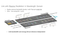
One of the biggest benefits photonics brings to petascale systems (a quadrillion calculations per second)—or even exascale systems (a quintillion calculations per second)—is its potential to move significantly more communication bandwidth within the system.
Moving data within an electrical domain is limited today because high-bandwidth communication “has a lot of loss, which requires exponentially more power to move increasingly more data,” says Bergman. “The reason to move to the optical domain is so we can do it with better energy efficiency—move the data with much lower energy consumption per bit over distances. And within each wire and pin on a chip, we can insert more bandwidth because photons are fundamentally bosons and won’t interfere with each other.”
Electrical systems densely packed together tend to produce crosstalk, interference, and other challenges. But within the optical domain, data can be modulated on different colors, wavelengths, or channels and all co-propagate within the same wire, fiber, or waveguide—and not interfere with each other. It enables squeezing more bandwidth per unit area per unit length for the chip.
“Optics offers two advantages here: We can have very high bandwidth densities—on the order of multiple terabits per millimeter,” says Bergman.2 “It also enables energies below picojoule per bit moving data over hundreds of meters or kilometers.”
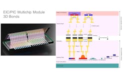
The challenge? Co-packaging or co-integrating these photonic chips with the electrical side, compute and memory, and other components at the edge of the computing system.
One way to deal with it is to codesign the optical links with the electronics in the most efficient way possible. “On the optical side, lots of wavelengths are available,” Bergman says. “They’re generated by an optical comb—a single laser can generate upward of 100 different colors at the same time with high precision.”
It begs the question: What’s the right data modulation frequency for each one of these wavelength channels to match the right data frequency that exists on the electrical side of that interface?
“These are important design questions,” says Bergman. “Others are related to the packaging. A photonic chip is made of silicon, so it looks just like an electrical chip. How do we co-package it so it interfaces with the electronic side? There are different ways to enhance the integration, such as 3D integration or even monolithic integration where the photonics and electronics exist within the same chip together.”
Beat the co-package heat
The research community and industry are asking questions about how to assemble these different technologies—photonics and electronics—together in the same heterogeneous package. Two of these key questions involve heat: How do we cool the package? And how do we maintain a certain temperature for optimal performance?
Photonics is a thermally sensitive technology, and “if the temperature of the photonic chip changes, its index of refraction changes,” explains Bergman. “We need to be able to adapt the photonic chip to temperature shifts—because temperature changes come from both the surrounding environment and the electrical side of the interface.”
In a three-dimensional (3D) package, heat generated on the electrical side can affect the performance of the optical chip, so it’s crucial to understand the thermal environment and compensate/design for it.
“We approach this in several ways,” Bergman says. “One is closed-loop circuitry that maintains the operation point of the photonics—even if the temperature changes. Another approach is to design the photonics to be as athermal as possible.”
These approaches inherently compensate for changes in temperature. “One material changes its temperature in one direction with the index of refraction, while the other one changes in the opposite direction—and it provides an inherent robustness we can design into the photonics,” Bergman adds.
Electronics, you’re the problem
Zooming out a bit, deep inside systems today “we have very good electrical connectivity in 3D, and the electrical chips between memory and the graphics processing units (GPUs),” says Bergman.
While this connectivity is good in terms of energy consumption and bandwidth, the problem with electronics is that when you need to move the data across the system—it costs a lot of in terms of energy, and the bandwidth can drop by as much as two orders of magnitude.
Bringing photonics right into the chip like an interface can potentially flatten communications across the entire system to eliminate the two-orders-of-magnitude taper that currently exists within systems completely.
“It will greatly accelerate the execution time of the application and the way we architect the systems to begin with,” says Bergman. “Potentially putting photonics within systems isn’t just a technology replacement, it will allow us to accelerate the performance of AI systems by orders of magnitude of what we’re capable of today—while maintaining the energy consumption. We can bend the curve on the energy consumption.”
An inflection point
We’ve reached an inflection point where photonics is still more costly than today’s electronic interconnect infrastructure—because manufacturing and the entire semiconductor ecosystem is much more mature than photonics.
“Companies want to commercialize and deploy these systems but, while energy and performance are important, cost ultimately rises to the top in real systems and projects. So we’re in a catch-22 situation: Can we bring photonics to a full manufacturing modality so there’s large volume to eventually drive costs down?”
Bergman is optimistic we’re getting there, because vendors on the computing side either have or are exploring a program in co-packaged optics/photonics and so it’s indeed on the horizon. “But we’re not quite there yet,” she says.
On the horizon
Photonics will clearly enable extreme-scale computing and beyond. For the electrical version of connectivity’s scaling will mean “we’d essentially need a nuclear power plant for the system’s power consumption,” says Bergman. “This is why it’s important to end the energy consumption curve and enable the scalability of future systems.”
Bergman and colleagues are also working on integrating flexibility into communication systems beyond interconnects to ensure switches are also wavelength-selective to enable systems to adapt to the nature of the communication of a particular application.
“This flexible, adaptable interconnectivity is another exciting area we’re working on, and another one is increasing the bandwidth beyond the wavelength domain—exploring the spatial/modal domain, so for every wavelength you can also have orthogonally independent spatial modes within that color or wavelength,” Bergman says. “When it increases, it’s a wave that increases the bandwidth density even further.”
FURTHER READING
1. A. Rizzo et al., Nat. Photon., 17, 781–790 (Jun. 2023).
2. A. Rizzo et al., IEEE J. Sel. Top. Quantum Electron., 29, 1–20 (Feb. 2023).
About the Author

Sally Cole Johnson
Editor in Chief
Sally Cole Johnson is Laser Focus World’s editor in chief, and she has more than 25 years’ experience as a science and technology journalist. She specializes in physics and semiconductors, and wrote for the American Institute of Physics for more than 15 years, and also covered theoretical physics and neuroscience for the Kavli Foundation, and complexity for the Santa Fe Institute. Johnson has also written extensively about military embedded systems, high-performance computing, software-defined networks, and infosec.
When she isn’t writing about optics, photonics, or quantum advances, you can find her outside in northern NH in the garden with birds landing in her hand or heading for the mountains with her bike, skis, or crampons and ice axe.