First broadband optical metalens also focuses arbitrary polarization states
Optical metalens technology, usually in the form of a nanoform metasurface fabricated on a flat optical substrate, has been often covered by Laser Focus World, including in the form of a camera lens, a stretchable lens, a doublet, and a microscope objective equivalent. One of the most interesting aspects of some forms of metasurface lens is that they are aimed at replacing a complicated optical component with a single, mass-producible flat element. Thus, for example, a bulky precision microscope objective could conceivably be replaced by a single small patterned glass plate.
However, one of the big problems of metasurfaces is that they are, in their most straightforward form, monochromatic. As a result, broadband metasurface imaging lenses would seem to be impractical. One compensating approach, in which a trichromatic red-blue-green metasurface lens was created, at least allows color imaging, although three narrowband light sources would have to be used rather than the usual broadband source.
True broadband metasurface lens
Now, researchers at Columbia University (New York, NY) have created a true broadband metasurface lens—with the added feature that it focuses arbitrary polarization states, including ordinary unfocused light.1 The lens is fabricated using standard computer-chip fabrication technologies, meaning that it could be mass-produced.
"The beauty of our flat lens is that by using meta-atoms of complex shapes, it not only provides the correct distribution of delay for a single color of light but also for a continuous spectrum of light," says Nanfang Yu, an associate professor of applied physics. "And because they are so thin, they have the potential to drastically reduce the size and weight of any optical instrument or device used for imaging, such as cameras, microscopes, telescopes, and even our eyeglasses. Think of a pair of eyeglasses with a thickness thinner than a sheet of paper, smartphone cameras that do not bulge out, thin patches of imaging and sensing systems for driverless cars and drones, and miniaturized tools for medical imaging applications."
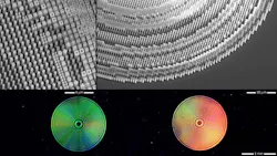
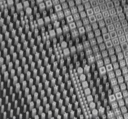
The Columbia metasurface lens was designed to work over the 1.2 to 1.7 µm wavelength range. The nanoscopic surface features of the lens are complex indeed, as seen in the microscopic images of the lens surface."Our design algorithm exhausts all degrees of freedom in sculpting an interface into a binary pattern, and, as a result, our flat lenses are able to reach performance approaching the theoretic limit that a single nanostructured interface can possibly achieve," Adam Overvig, one of the study’s co-lead authors and also a doctoral student with Yu, says. "In fact, we've demonstrated a few flat lenses with the best theoretically possible combined traits: for a given metalens diameter, we have achieved the tightest focal spot over the largest wavelength range."
The flat lenses currently do not have optimal efficiency because a small fraction of the incident optical power is either reflected by the flat lens, or scattered into unwanted directions. The team is optimistic that the issue of efficiency is not fundamental, and they are busy inventing new design strategies to address the efficiency problem. They are also in talks with industry on further developing and licensing the technology.
Source: https://engineering.columbia.edu/press-releases/nanfang-yu-flat-lens
REFERENCE:
1. Sajan Shrestha et al., Light: Science & Applications (2018); doi: 10.1038/s41377-018-0078-x.
About the Author
John Wallace
Senior Technical Editor (1998-2022)
John Wallace was with Laser Focus World for nearly 25 years, retiring in late June 2022. He obtained a bachelor's degree in mechanical engineering and physics at Rutgers University and a master's in optical engineering at the University of Rochester. Before becoming an editor, John worked as an engineer at RCA, Exxon, Eastman Kodak, and GCA Corporation.


