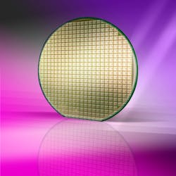
DSI to debut thin-film face metallization and solderable coatings at SPIE DSS 2014
A line of thin-film face metallization and solderable coatings on a wide variety of substrates are typically used for hermetic sealing of sensitive packages in infrared (IR) detectors and cameras, focal-plane arrays, and other sealed sensors/detectors. The coatings can be combined with antireflection (AR), bandpass, or precision custom coatings from ultraviolet (UV) to longwave IR (LWIR) wavelengths. The company can also pattern the coatings at wafer scale to be compatible with wafer-level packaging operations, and can produce patterned optical filters up to 200 mm in diameter. An enhanced photolithography capability provides view or detection in multispectral imaging tasks by fusing information from different wavebands. Advanced patterned and multilayer thin-film coating applications include unmanned aerial vehicle (UAV) overhead reconnaissance, satellite imaging, CCD, and CMOS filter arrays, reticles, and inspection.
SPIE DSS booth number: 743
To Learn More:
Contact: Deposition Sciences (DSI)
Headquarters: Santa Rosa, CA
Product: Thin-film face metallization and solderable coatings
Key Features: Wafer-scale patterning capability and an enhanced photolithography capability
What DSI says:
View more information on the company's thin-film face metallization and solderable coatings.
Locate a vendor or system integrator in our Buyer's Guide.
Share new products that you think are particularly interesting or helpful by contacting Lee Dubay, Associate Editor, Laser Focus World.
