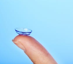
Scientists from the University of South Australia's (UniSA's) Future Industries Institute (FII) have successfully completed 'proof of concept' research on a polymer thin-film coating that conducts electricity on a contact lens, with the potential to build miniature electrical circuits that are safe to be worn by a person. UniSA researcher Drew Evans says the technology could provide one of the safest methods to bring people and their smart devices closer together.
RELATED ARTICLE: Contact lens could create virtual display
"Building on the technologies we pioneered in thin film coatings for the development of the world's first fully plastic car mirrors, we have been working on the development of conducting polymers with a UK partner that specialises in contact lenses," says Evans. "We have always known that our film coating technologies had potential for many applications and now we have taken that a step further by proving that we can make biocompatible, conducting polymers at the nanoscale and grow them directly on a contact lens."
Evans continues, "The fluids in the eye provide markers of a person's health, so our goal now is to build electrical sensors on a contact lens from our polymers to sense in real time a person's well-being. The next big leap is to develop complementary technologies to read the information transmitted by the conducting polymers." Evans says this research has brought personal, wearable computer technologies one step closer.
The complete proof of concept research results have recently been published in ACS Applied Materials and Interfaces.
SOURCE: University of South Australia; http://www.unisa.edu.au/Media-Centre/Releases/UniSA-puts-all-eyes-on-next-generation-electronics/#.VrgtX-anG7A
About the Author

Gail Overton
Senior Editor (2004-2020)
Gail has more than 30 years of engineering, marketing, product management, and editorial experience in the photonics and optical communications industry. Before joining the staff at Laser Focus World in 2004, she held many product management and product marketing roles in the fiber-optics industry, most notably at Hughes (El Segundo, CA), GTE Labs (Waltham, MA), Corning (Corning, NY), Photon Kinetics (Beaverton, OR), and Newport Corporation (Irvine, CA). During her marketing career, Gail published articles in WDM Solutions and Sensors magazine and traveled internationally to conduct product and sales training. Gail received her BS degree in physics, with an emphasis in optics, from San Diego State University in San Diego, CA in May 1986.