Magneto-optics enable waveguide-mode switch
Incorporating news from O plus E magazine, Tokyo
HYOGOA group at the Material Science Division of the Electrotechnical Laboratory has developed a magneto-optic waveguide on a gallium arsenide (GaAs) substrate and has confirmed that waveguide-mode switching is possible. The technology can be used to create optical integrated circuits containing optical isolators, optical circulators, and other parts joining the optical elements and waveguides within a semiconductor system.
The group used cadmium manganese telluride (Cd1-xMnxTe) as the magneto-optical material. This material, which has the same crystalline structure as GaAs, is a dilute magnetic semiconductor with extremely strong magneto-optical properties. The magneto-optical efficiency index rivals that of the well-known magneto-optical material yttrium iron garnet.
There is a 12% gap between the lattice constant of Cd1-xMnxTe and that of the GaAs substrate, so it is difficult to make a high-quality film. Therefore, a buffer layer of CdTe must first be created on top of the substrate before the waveguide layer is grown. However, a Te and Ga compound can form when the CdTe layer is grown, creating defects that greatly reduce the characteristic properties of the waveguide. Thus, a one-atom-thick layer of pure Cd is created before the Te is added to prevent defect formation. Once the CdTe buffer layer is formed, a layer of Cd0.7Mn0.3Te is grown on top of it, then a layer of Cd0.85Mn0.15Te. The higher the concentration of Mn, the higher the index of refraction. Thus, the first Mn-containing layer serves as the core, and the second as the cladding layer.
The resulting waveguide has an optical loss of less than 4 dB/cm at a wavelength of 790 nm. This is very low compared to the figure of 65 dB/cm achieved when the defect-reduction treatment is not performed while growing the CdTe layer. Although the magneto-optic efficiency index is lower than that for a bulk crystal, it is sufficient for commercial applications.
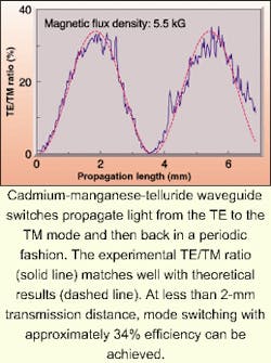
The group has conducted waveguide-mode switching experiments using this device. In waveguide-mode switching, energy is exchanged between the characteristic modes of the waveguide, the TE mode and the TM mode, corresponding to the rotation of the polarization plane. It is a fundamental phenomenon that can be exploited to create waveguide-type optical isolators and optical circulators.
In the experiment, 790-nm light irradiates the waveguide and excites the TM mode. Of the small amount of scattered light that leaks out from the waveguide, only the TE component is measured. When no magnetic field is applied, light cannot be detected. It can be deduced that only the TM mode is transmitted. When a magnetic field of 5.5 kilogauss (kG) is applied in the direction of the traveling light, periodic streaks of light can be seen. Such a phenomenon occurs because part of the TM-mode light is being converted to the TE mode (see figure). This is the first time that waveguide-mode switching has been accomplished using a semiconductor substrate.
The switching efficiency must be improved before considering commercial applications, but higher efficiencies should be possible by phase matching. The waveguide here was used in its two-dimensional thin-film state. Since the waveguide is made of a semiconductor material, a one-dimensional version can be easily made. In addition, the 5.5-kG magnetic-flux density can be created using a small permanent magnet of the kind already used in optical isolators in fiberoptic communications systems.
Courtesy O plus E magazine, Tokyo

