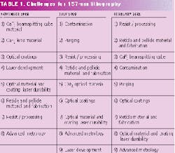
Challenges remain for 157-nm lithography
JAMES MCCLAY, THOMAS FAHEY, and MATTHEW LIPSON
A program begun in 1998 by Silicon Valley Group (now ASML) identifies challenges and risks associated with the development of 157-nm lithography and aims to establish partnerships with industry experts to find suitable solutions. These partnerships involve collaboration on all aspects of 157-nm lithography, including the infrastructure needed to support the exposure tool—for example, photoresists, photomasks (reticles), and advanced metrology. The project has led to the discovery of new issues, while at the same time overcoming earlier challenges.1
The relative importance of the challenges and risks has changed since 1998 (see Table 1). Progress of broadband laser development has been so significant, for example, that it has been taken off the risk chart altogether. Major progress also has been made with purging and contamination, and these areas have therefore become less crucial.
Photoresist and resist processing
Most equipment users rank photoresist (often called resist) and resist processing as the highest-risk areas in the overall 157-nm endeavor. Customers require that lithographic tools pass an acceptance test procedure that includes demonstration of resolution, linewidth control, and overlay. Resist performance plays an important role in lithographic equipment verification as well as in users' device development.
Significant progress has been made with regard to resist development. In one example, 157-nm patterning achieved 80-nm lines and spaces at an exposure dose of 2.75 mj/cm2.2 The real issue, however, is timing; thus, resist heads to the top of the risk chart. The industry needs to have a well-demonstrated resist process in place by 2003 to support the introduction of 157-nm systems. It is likely that problems with 157-nm resist will be overcome, just as they have at 193 nm.
Pellicle material and fabrication
Anyone who has followed the saga of pellicle development is now familiar with the highs and lows that have plagued the effort. In the past two years pellicle problems appeared to be lessening, only to become an issue again.
The current situation, which could change pending developmental results, shows significant problems with obtaining "soft" pellicle material capable of withstanding laser damage. Investigations into "hard" pellicles have been more successful, but there are limitations with regard to pellicle thickness. Lithography equipment manufacturers are setting these limits because of the potential for optical aberrations and the resulting image degradation. Depending on the lithography equipment, the type of optical design, and the mounting configuration (horizontal vs. vertical), the thickness limitation on pellicles ranges between 300 and 800 µm.
The dilemma is that, while equipment manufacturers demand a limitation on the thickness of hard pellicles, pellicle manufacturers are faced with mechanical aspect ratios (size vs. thickness) that cause problems not only with the manufacture of the pellicle itself, but also with mounting of the pellicle to the reticle.
Couple all these problems together and pellicles move to near the top of the risk chart. Equipment manufacturers are now investigating a design for a so-called no-pellicle solution. This is a formidable challenge that requires not only protecting the reticle from particulate contamination as it resides within the lithography exposure system, but also protecting it in transit from the reticle manufacturer to the tool.
Controlling particles to a level that supports lithography with 70-nm design rules is not a simple task. It is further complicated by the fact that particulates must now be classified as hard defects, which print readily and affect yield. The reticle itself needs to be handled as an optical element with an emphasis on the molecular contamination that can affect overall transmission, and can lead to dose nonuniformity.
Calcium fluoride
Few materials are able to transmit 157-nm energy, exhibit the proper optical properties, and also survive the effects of 157-nm laser irradiation. Calcium fluoride (CaF2) is one optical material that can. It was incorporated into lithography equipment to a very limited degree with certain optical designs at 248 nm, then became more prevalent when the wavelength shifted to 193 nm. Now it is the material of choice for 157 nm. Key specifications revolve around material birefringence, homogeneity, and absorption at 157 nm.
A material that tests well for absorption at 193 nm may absorb significantly at 157 nm. It is not sufficient to specify homogeneity only as a lumped value; instead, it must be specified for individual Zernikes. Acceptable values of specific Zernike coefficients are dependent on the optical design sensitivities and are specific to how each is accommodated during the optical-system fabrication, test, and alignment. All these values are also coupled with the need for low birefringence. The net result is that nothing can be taken for granted and that every piece of CaF2 slated to be used within the 157-nm optical train must be thoroughly categorized and evaluated prior to acceptance and use.
All suppliers of CaF2 continue to make significant investments in new furnace technology, some in collaboration with lithography-equipment suppliers. They are also making investments in the metrology needed to test and categorize the material. Both Canon (Utsunomiya, Japan) and Nikon (Tokyo, Japan) have made announcements about building dedicated CaF2 facilities. ASML continues to work closely with Schott (Duryea, PA), Bicron (Newbury, OH), Corning (Corning, NY), and American Crystal (Fremont, CA).
While significant progress has been made in material quality, furnace yields for both 193-nm and 157-nm high-quality optical material are significantly lower then expected, which shows up as material shortages. It is likely that, as new capacity from improved furnaces comes on line and as the learning process continues, the CaF2 situation will substantially improve over the next 12 to 18 months. With the continuing development, it is expected that CaF2 will leave the risk chart during the next 18 months.
Contamination and purging
As the development of 157-nm technology progresses, the importance of controlling purging and contamination becomes much more critical. Throughput loss for oxygen and water vapor in the gas surrounding the optics can be defined as follows: the presence of diatomic oxygen at a concentration of 0.6 part per million causes a 1% optical loss per meter for light at 157 nm; so does the presence of 1.3 parts per million of water vapor. Strong optical absorption by oxygen and water vapor in air can be alleviated by purging the optical path with nitrogen gas.
Oxygen and water do not negatively impact the lifetime of the optics. In fact, oxygen mitigates the effect of certain molecular contaminants. Design of a purge system that encompassed the complete optical path (particularly in the open regions of the tool around the moving wafer and reticle stages) required designs based on quantitative models of flow dynamics.
With respect to molecular contamination of optics, no quantitative model existed before the 157-nm program was instituted. Losses from molecular contamination can be categorized as absorption loss, dielectric detuning, and uniformity loss. The approach to controlling the molecular contamination rate of optics has been twofold: quantify the rate at which various molecular species contaminate optics at 157 nm, and quantify the sources of the molecular species. The first permits the setting of a maximum allowable level of molecular contamination in the tool; this, coupled with the second, makes possible the selection of proper materials to build an exposure tool that will not be adversely affected by contamination during its working lifetime.
Hydrocarbons and silicones both contaminate optics. Hydrocarbons are molecules predominantly composed of carbon and hydrogen, but they may include oxygen, sulfur, nitrogen, chlorine, bromine, and iodine (among other atoms). Silicones, tightly defined, are molecules with a silicon-oxygen-based backbone, but for our purposes loosely also include the family of silanes.
Molecular contamination can be placed into two categories: actinic and thermal. Actinic contamination refers to the tendency of a material to outgas when exposed to light, specifically 157-nm radiation. Thermal contamination refers to outgassing under ambient conditions. Various sources of hydrocarbon and silicone contamination include actinic and thermal, adhesives and cements, paints, plastics, caulking, lubricants, primers, and fingerprints. The general conclusion drawn from this list is that the only materials that do not contribute to molecular contamination of 157-nm optics are metal, glass, and calcium fluoride (assuming that they have been adequately cleaned via an approved method).
The contamination of optics follows a two-step process. First, hydrocarbon or silicone contamination adsorbs from the vapor phase onto the surface of the optic. Second, the molecule absorbs a photon of 157-nm light and undergoes one of the following chemical reactions:
- Hydrocarbon plus 157-nm light produces graphite
- Hydrocarbon plus oxygen and 157-nm light produces volatile alcohols
- Graphite plus oxygen and 157-nm light produces volatile alcohols
- Silicone plus 157-nm light produces silicon dioxide (glass)
- Silicone plus oxygen and 157-nm light produces silicon dioxide
The effect of contamination on an optical surface is twofold. It degrades optical performance by absorbing photons (the dominant effect of hydrocarbon contamination) and by detuning dielectric coatings (dominant for silicone contamination). For example, graphite results in a 1% loss per 0.5-nm deposited thickness, while silicon dioxide results in a 1% loss per 1.3-nm thickness.
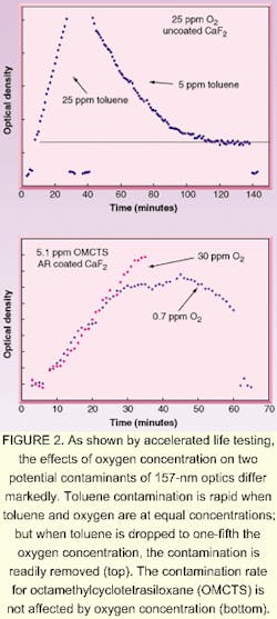
Of significant importance is that the addition of controlled oxygen levels into the purge gas, when coupled with 157-nm photons, actually removes hydrocarbon contamination from the optical surfaces. This process has little or no effect on silicone induced contamination, however.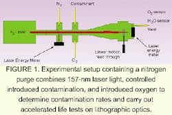
Data from these experiments, combined with the knowledge of oxygen levels achieved inside the lithography tool, help to establish maximum levels of contamination relative to purge flow rates. Quantification of outgas rates and identification of outgas components for the various materials needed in the tool are then derived to support the system design specifications.
The outgas test varies, depending upon the conditions in which the material is used. An adhesive that is exposed to laser light is tested for actinic outgas; a paint that sees no laser light is tested only for thermal outgas; and materials, such as gloves, used in the handling of parts are tested by a wipe test (see Table 2).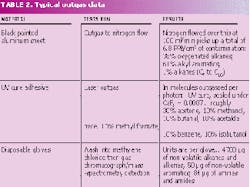
Coupling data from controlled contamination tests with data from material outgas testing allows both a qualitative and quantitative assessment of the system design. This assessment provides assurance that the exposure tool performance will not be adversely affected by contamination over its lifetime. Work still needs to be done to address remaining challenges and to position 157-nm optical lithography as an effective and practical technology. The 157-nm development effort continues to gain momentum and demonstrates the industry's interest in finding an evolutionary optical solution.
ACKNOWLEDGMENT
The authors would like to thank Carol Miklus for her help on this article.
REFERENCES
- T. Fahey, J. McClay, M. Hansen, B. Tirri, and M. Lipson, SPIE Post Paper, SVGL 157-nm Lithography Technical Review, February 2001.
- Laura Peters, Resist Developers Try to Beat the Clock, Semiconductor International, 24 (February 2001).
James McClay is vice president, 157 Program; Thomas Fahey is program manager, 157 Program; and Matthew Lipson is principal engineer at ASML (formerly Silicon Valley Group), 77 Danbury Road, Wilton, CT 06897; e-mails: [email protected], [email protected], and [email protected].