Modified silica transmits vacuum UV
Charlene Smith
The wavelength of light used for photoresist exposure in leading-edge optical lithography has evolved from longer-wave ultraviolet (UV) to the deep-UV wavelengths of 248 and 193 nm. In the near future, the use of the vacuum-UV wavelength of 157 nm is expected to produce lithographic feature sizes of 70 nm. As the exposure wavelength shortens, the choice of optical materials becomes more limited. Many glasses transmit light at the g-line of the mercury-arc spectrum (436 nm), and in fact, a typical g-line lens may contain as many as 15 different glasses in its lens elements.1 The choice of materials in the deep and vacuum UV becomes restricted to wide-bandgap materials. In principle, these materials include crystalline quartz, synthetic silica glass, and fluoride crystals. Crystalline quartz is not used for imaging applications because of its natural birefringence and relatively low transmission as a result of impurities. Amorphous silica glass, however, is an ideal material for these demanding applications, bringing high transmission and isotropic properties. Recently developed modifications to silica glass allow lithographers to use the material as a substrate for photomasks that transmit well at 157 nm.
The essential silica
Silica glass (silicon dioxide, or SiO2) has the same bonding properties as crystalline quartz but lacks the crystalline order of quartz. The general SiO2 structure can be described as a network of SiO4 tetrahedra bonded at the corners. In contrast to crystalline quartz, silica glass has these units randomly oriented with respect to each other. The amorphous nature of the glass does not affect the bandgap, so that quartz and silica glass both have roughly a 9-eV bandgap. Extrinsic contaminants such as metal ions, hydroxyl linkages, or chloride introduce states in the gap and reduce the transmission of silica glass at wavelengths shorter than 185 nm.
Excimer-grade illuminator and projection-lens optics for lithography at 248- and 193-nm wavelengths are usually fabricated from very pure synthetic silica glass, with perhaps a few elements of single-crystal calcium fluoride (CaF2) included for color correction owing to the bandwidth of the laser source. The photomaskthe thin flat element on which the circuit-pattern information is containedis also synthetic silica glass. The choice of silica for the photomask application is directly related to its favorable optical and mechanical properties, including low thermal expansion and ease of polishing over a large 6 x 6 in. area.
The photon energy of 157-nm light is roughly 7.8 eV, and as such the number of materials that are sufficiently transparent at this wavelength is limited. The single-crystal fluorides (lithium, sodium, calcium, and magnesium fluorides) have the wide bandgap necessary for transmission at this wavelength. For several reasons, CaF2 is the material of choice for 157-nm illuminator and projection-lens optics; aside from the necessary transmission, these reasons include the material's cubic crystal structure, availability, and relative ease of polishability.
However, the use of CaF2 for the photomask material presents something of a problem in that it has a high coefficient of thermal expansion (19 ppm/K)roughly 40 times that of silica. The high expansion presents problems during the electron-beam mask writing and handling procedures; consequently it would be desirable to use silica for the photomask material. A photomask material must have a transmission of greater than 80% for a 6.35-mm thickness; by a proper choice of preparation conditions, this can be achieved in silica glass. In fact, it is possible to achieve sufficiently high transmission for a photomask application in silica glass at 157 nm and retain the physical properties that are so amenable to lithography work.
Fabricating silica
The requirement for extremely high transmission at the deep and vacuum-UV wavelengths necessitates that the glass be very pure, particularly with respect to metal contamination. Consequently, the lithography excimer-grade silica glass that is currently used in the industry for photomasks and illuminator and projection optics at 248 and 193 nm is not melted from mined quartz, but is typically prepared by flame hydrolysis or chemical deposition. In such a process, introducing a purified silicon-containing liquid feedstock (silicon tetrachloride, for example) into a flame (a fuel such as hydrogen or methane combined with oxygen) produces very pure, amorphous silica glass. The combustion process yields SiO2 that is either directly deposited into a large boule or collected as soot particles and subsequently formed into the final rough part. As a consequence of the combustion process, the glass will typically contain some amount of hydroxyl (OH; often referred to as water although it appears to be SiOH groups) and molecular hydrogen.
For the photomasks and optics to be used at wavelengths longer than 193 nm, the presence of SiOH is benign; that is, it does not diminish transmission at the wavelengths of interest or otherwise interfere with the desired properties of the glass. As it turns out, the incorporation of hydrogen is a vital element in the dynamic use of silica with excimer laser irradiation at wavelengths above 193 nm.2
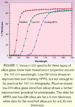
The presence of SiOH does not contribute to absorption at 193 nm, but as shorter wavelengths are approached, the presence of hydroxyl decreases transmission (see Fig. 1). Compared are the vacuum UV spectra of a high-OH silica glass appropriate for use at wavelengths above 193 nm (Corning HPFS ) and a low-OH or dry silica. While the transmission of the so-called dry glass is higher than the wet glass, it does not meet the requirement of greater than 80% transmission for a 6.35-mm thickness. This transmission can be achieved by fluorine doping of dry glass. The low-OH, fluorine-doped silica glass is often referred to as modified silica.3
Whereas silica for use at 248 or 193 nm is most typically obtained from the direct-deposition method, it is necessary to use a soot-deposition process, followed by drying and doping to prepare modified silica for use in 157-nm photomasks. In the soot consolidation process, high-purity silica soot particles are generated from the flame. The soot is collected and chemically dried at a high temperature. The dry soot is then exposed to a fluorine atmosphere and consolidated into a dense solid body. Different levels of fluorine can be incorporated into the glass, depending on the process conditions used. The amount of fluorine incorporated into the part will have an effect on the mechanical and optical properties. The hydroxyl content of the glass made by this method can be less than 1 part-per-million OH by weight.
In high-OH glasses, hydroxyl is incorporated into the structure as SiOH, with the silicon atom bonded to three other oxygen atoms. Fluorine is similarly incorporated into the modified silica structure as SiF. As with the hydroxyl unit, this bonding arrangement excludes any possibility of fluorine out-diffusion, which would result in a change of the glass properties with time.
Effects of fluorine
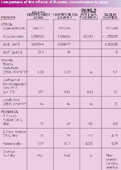
The effect of fluorine concentration on the mechanical and optical properties of modified silica has been studied.4 Young's modulus, shear modulus, and coefficient of thermal expansion all decrease linearly with increasing amounts of fluorine. Thermal conductivity and specific heat are largely unaffected by the addition of fluorine. The index of refraction of silica also decreases linearly with increasing fluorine. Optical and mechanical properties of modified silica containing 0.8 wt% fluorine are compared to those of lithography excimer-grade, high-hydroxyl silica (see table). The absolute refractive index at 157 nm was measured only on the 0.8 wt% fluorine-concentration composition.5 Index data measured through the visible and UV were used to fit to the Sellmeier equation, yielding the estimate of the change in index as a function of fluorine concentration at 157 nm. Also presented are data for CaF2.
Such property data demonstrate that the compositional change necessary to affect high transmission in the vacuum UV (using modified silica) does not negatively impact other desirable properties of the glass for use in photomasks. The coefficient of thermal expansion and thermal conductivity are essentially unchanged over the range of fluorine concentrations examined from the familiar excimer-grade silica material currently in use in the lithography industry. Because of index dispersion, the refractive index of modified silica at 157 nm is considerably higher than that for lithography-grade high-OH silica at 193 nm. As a second point of comparison, CaF2 has an index of refraction of 1.56 at 157 nm. The high coefficient of thermal expansion in CaF2 is somewhat offset by its large value for thermal conductivity. It has been found, however, that CaF2 exhibits an order-of-magnitude-larger distortion during mask writing as compared to fused silica.6
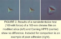
The data suggest that insertion of modified silica into mask fabrication lines would be straightforward and relatively invisible to the process. This possibility was examined by conducting polishing, film deposition, and film adhesion tests. It was possible to polish modified silica to 0.20-nm root-mean-square roughness under the same chemical mechanical conditions used to produce 0.17-nm surfaces on high-OH excimer-grade silica. Chrome deposition was accomplished by cleaning photomask substrates having high OH and modified silica compositions in sulfuric acid/peroxide solution and mask detergent, followed by drying and metal deposition by sputtering. The as-made films were indistinguishable and were similarly resistant to indentation and scratch testing using a nanoindenter (see Fig. 2). Modified silica in its optical and mechanical characteristics is essentially equivalent to current photomask materials.
An issue not addressed here is lifetime of the modified silica mask under 157-nm laser exposure. Mask lifetime requirements are not as stringent as those of other optical elements, since the mask is a disposable item.7 However, the material does need to maintain high transmission over the course of several hundred million pulses at exposure fluences of 0.1 to 0.2 mJ/cm2/pulse. In 1999, workers at the Massachusetts Institute of Technology Lincoln Laboratory (Lexington, MA) reported at least one type of modified silica meeting the criteria for photomask lifetime.8 Improvements in the material have been made by potential suppliers, yielding an appropriate material for use as a 157-nm optical element.9
ACKNOWLEDGMENTSThe author is pleased to recognize her collaboration with Lisa A. Moore, Coby Miller, Roger Welch, and Michelle Pierson-Stull, all of the Glass and Glass-Ceramics Core Technology Group at Corning Incorporated. The support of Brad Ackerman is also gratefully acknowledged. We appreciate the work of John Burnett of NIST in measuring absolute index and Bruce Smith of RIT for the coating work.
REFERENCES
- Introduction to Microlithography, Second Edition, L. F. Thompson, C. G. Wilson, and M. J. Bowden, eds., American Chemical Society (Washington, DC; 1994).
- C. M. Smith, N. F. Borelli, and R. J. Araujo, Appl. Opt. 39, 5778 (2000).
- C. M. Smith and L. A. Moore, Proc. SPIE 3676, 834 (1999).
- L. A. Moore and C. M. Smith, Proc. SPIE 3873, 393 (1999).
- J. Burnett, R. Gupta, and U. Griesmann, 157-nm Tech. Data Review, Sematech Sponsored Symposium (Waltham, MA; Nov. 17-19, 1999).
- J. Chang et al., Proc. SPIE 3676, 756 (1999).
- C. M. Smith and B. G. Ackerman, Solid State Tech. 44, 111 (2001).
- V. Lieberman et al., J. Vac. Sci. Tech. B 17, 3273 (1999).
- C. M. Smith and L. A. Moore, Proc. SPIE 4346, 110 (2001) and references therein.
CHARLENE SMITH is a research associate at Corning Incorporated, SP FR 03, Corning, NY 14831; e-mail: [email protected].


