Filters that select certain electromagnetic wavelengths and reject others can be constructed from arrays of metallic features with dimensions somewhat less than the wavelength, and feature widths finer still. Such filters are easily made for the microwave region and, using standard photolithographic techniques, for the far-infrared region. For shorter wavelengths, however, such structures can only be made using more expensive or experimental lithographic techniques such as x-ray, e-beam, and extreme ultraviolet. Now, researchers at Harvard University (Cambridge, MA) are using a nonstandard but simple and low-cost form of lithography—so-called soft lithography—to make wavelength-selective surfaces for the mid-infrared.1
Soft lithography uses an elastomeric polymer element to transfer a pattern. The researchers chose near-field contact-mode lithography to pattern arrays of aluminum rings on windows of silicon or single-crystal calcium fluoride (CaF2) over areas of up to 4 cm2 or more. A phase mask serving as a stamp is made by casting a polymer on a patterned master containing features 400 nm high. The stamp is brought into contact with a 200-nm layer of photoresist ("resist") coated on a substrate. Broadband (365 to 436 nm) ultraviolet light is passed through the stamp to expose the resist. For CaF2, a positive resist is used, resulting in post-development features corresponding to the edges of the features on the stamp. For silicon, a negative resist results in trenches on the resist surface.
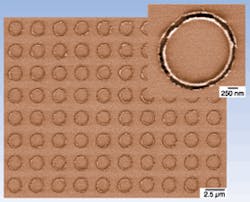
Arrays of rings were printed. A stamp having 950-nm circular depressions produced rings in positive resist 850 nm in diameter on CaF2. Depressions 2.15 µm in size produced 1.85-µm-diameter rings on CaF2 (see figure). Using negative resist on silicon resulted in trenches of 2.15-µm outer diameter and 1.45-µm inner diameter from 2.15-µm depressions. A post-exposure bake, aluminum deposition, and resist lift-off produced arrays of metallic rings with a ratio of feature size to linewidth of approximately 10.
A Fourier-transform infrared spectrometer was used to measure the spectral transmission of the samples. The 850-nm rings on CaF2 exhibited a passband at 3.18 µm, close to the calculated value of 3.25 µm, while the 1.85-µm rings on CaF2 showed a passband of 7.07 µm, meshing with the theoretical prediction. A measured stop in transmission at 12.9 µm for the rings on silicon, however, did not agree with the predicted value of 16.9 µm. Hypothesizing that a thin oxide layer on the silicon could be altering the results, the researchers used an ellipsometer to check the surface, finding a 10-nm-thick oxide layer. Such a layer would reduce the effective refractive index of the silicon-air media from 2.5 to 1.91, bringing experimental results in line with theory.
Soft lithography using elastomeric stamps could be used to print similar features on curved surfaces as well. The main disadvantage of the technique, say the researchers, is that currently it can only print patterns consisting of closed loops, forbidding the fabrication of other interesting features such as crosses.
REFERENCE
- K. E. Paul et. al., Appl. Optics 40(25), 4557 (Sept. 1, 2001).
About the Author
John Wallace
Senior Technical Editor (1998-2022)
John Wallace was with Laser Focus World for nearly 25 years, retiring in late June 2022. He obtained a bachelor's degree in mechanical engineering and physics at Rutgers University and a master's in optical engineering at the University of Rochester. Before becoming an editor, John worked as an engineer at RCA, Exxon, Eastman Kodak, and GCA Corporation.
