Researchers at the Military University (Munich, Germany) have devised and tested a scanning positron microscope (SPM) that allows them to measure material defects with much higher resolution (defect concentrations on the order of 1 part per million) than either electron or optical microscopy, and that may find usefulness in the manufacture of semiconductor circuits and materials.1
The sensitivity of the SPM comes partially from the tendency of positrons to survive longer within material vacancies where the density of electrons available for mutual annihilation is small. Another sensitivity factor is due to the variance of positron lifetimes across different types of material defects. In addition, the ability to control incident positron energies further enhances the SPM measurement technique.
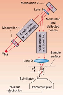
Actually, the first SPM step is to perform electron-beam microscopy of the surface of interest to map the structure and identify the areas to be scanned for defects. In their recently published work, the researchers described the device they designed to deliver positrons to the sample through the same optical column as the electrons in the previous step (see Fig. 1).
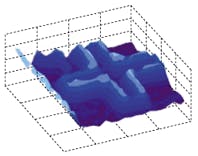
A primary factor that made the SPM design more challenging than simply aiming a different source through an electron-beam microscopy device was the much weaker typical flux density of positron sources (several orders of magnitude) compared with typical electron sources. The SPM design required a probe forming strategy focused on maintaining an adequate positron flux, as opposed to a typical, narrow probe aperture and permissible energy losses for electron beams. In addition, a large radiation detector was required to maximize the collection rate of signals from particle annihilations. The space between probe and sample also had to be as free of matter as possible to prevent data artifacts from annihilation of backscattering positrons.The sample that was tested consisted of a platinum pattern evaporated onto the silicon dioxide layer of a silicon wafer (see Fig. 2). Each pixel of the 20 x 20 pixel image required a 140-s positron-lifetime measuring time with the 30-mCi source of 22Na. Mean positron lifetime varied from 190 s in the platinum to 350 s in the silicon dioxide. In a subsequent experiment, SPM was also used to measure a 1.2-mm-long and 75-µm-wide scratch defect that had been placed in a gallium arsenide wafer using a diamond needle. In this case, in addition to accurately describing the visible (by optical microscopy) scratch mark, the SPM method also revealed an invisible plastic deformation just prior to the beginning of the visible scratch.
Now that the SPM concept has been demonstrated, the researchers hope to substantially increase the resolution of the technique by using an intense reactor-based positron source.
REFERENCE
- A. David, G. Kögel, P. Sperr, and W. Triftshäuser, Phys. Rev. Lett. 87, 7402 (Aug. 6, 2001).
About the Author
Hassaun A. Jones-Bey
Senior Editor and Freelance Writer
Hassaun A. Jones-Bey was a senior editor and then freelance writer for Laser Focus World.
