Silicon (Si) is transparent to light at infrared (IR) wavelengths longer than 1 µm. Because Si integrated circuits (ICs) are typically coated with opaque metal layers, techniques that image IC features through the back side of the wafer with IR light are valuable for inspection. Ordinary microscopes are limited to a resolution on the order of half a wavelength of light, or 0.5 µm for backside inspection of ICs—a limit far too coarse for today's lithographic feature sizes, which are reaching down to 0.13 µm.
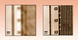
Researchers at the Photonics Center at Boston University (Boston, MA) have developed a microscope based on a solid immersion lens, or numerical-aperture-increasing lens (NAIL), that images at a numerical aperture (NA) of up to 3.4. The instrument has demonstrated a 0.23-µm resolution and has a theoretical spatial resolution of 0.14 µm. An almost-hemispherical section is placed in contact with the back of the wafer; the center of curvature of the hemisphere as seen from the outside coincides with the front wafer surface. Rays once refracted by the wafer surface now exit without refraction. A standard microscope system then images the IC features that rest at or near the center of curvature. An image taken by a state-of-the-art microscope with a 100X objective and without the NAIL (left) is poorly defined in comparison to an image taken with the NAIL in combination with a mere 10X objective (right). The features shown are from a static random-access memory device.
Two things could possibly be preventing the NAIL from reaching its theoretical resolution limit, says Selim Unlu, one of the researchers. Either the lines themselves are not as sharp as they could be (sloping sidewalls), or a very small air gap between the NAIL and wafer could be attenuating the higher-NA rays. The researchers, who have not yet tried hard to control the air gap or surface contamination, are preparing a precise sample made with electron-beam lithography to determine which is the cause of the lower resolution. "We think we can get down to sub 0.2-µm resolution," notes Unlu.
About the Author
John Wallace
Senior Technical Editor (1998-2022)
John Wallace was with Laser Focus World for nearly 25 years, retiring in late June 2022. He obtained a bachelor's degree in mechanical engineering and physics at Rutgers University and a master's in optical engineering at the University of Rochester. Before becoming an editor, John worked as an engineer at RCA, Exxon, Eastman Kodak, and GCA Corporation.
