Etching facets improves manufacturing of edge-emitting lasers
AL BENZONI, HANK BLAUVELT, MIKE NEWKIRK, JOEL PASLASKI, and ROLF WYSS
All laser diodes include an active layer that provides optical gain and a mechanism for providing optical feedback. For edge-emitting lasers, mirrors are typically formed by cleaving the wafer into bars and then depositing mirror coatings, as required, onto the cleaved facets. Because the optical mirrors are essential for operation, lasers fabricated in this manner are not functional until after the wafer has been cleaved into bars and the mirror coatings have been applied. The handling and testing of devices at bar level is a significant factor in the cost of edge-emitting lasers with cleaved facets.
An alternate approach is to form the mirrors by etching vertical facets. Mirror coatings are also applied at wafer level after etching. Using this approach, the lasers are fully functional at the wafer level. This allows for low-cost wafer probing of the devices to screen key laser operating parameters such as threshold currents/voltages, series resistance, lifetime versus current and voltage, center lasing wavelength, and wavelength spectrum. Producing facets through a wafer-scale etching process slightly increases the number of wafer fabrication steps, but greatly reduces the amount of back-end device handling at bar level and eliminates backside processing which results in yield improvements. And, without sacrificing reliability, etching facets also enables certain performance enhancements and minimizes packaging costs.
Fabrication process comparison
To highlight some of the manufacturing advantages of etched-facet lasers, the production steps can be compared to those of cleaved facet lasers (see table). The etched-facet fabrication process is being used in production at Xponent Photonics on both Fabry-Perot (FP) and distributed feedback (DFB) lasers.
Relative to typical cleaved facets, wafer-scale processing offers a number of significant handling advantages that help reduce costs and increase yields. With cleaved-facet lasers the n-contact is formed by lapping and polishing the wafer and depositing the n-contact metal stack on the backside. The backside process step requires handling of thinned wafers, which are fragile and susceptible to breakage. In addition, the cleaved-facet process also requires handling of laser bars for application of facet coatings. Facet-coating bars is a time-consuming process and requires great care to achieve environmentally stable performance. With cleaved facets the additional steps of backside processing, cleaving and bar-level facet coating are all needed before testing and evaluation of devices can take place prior to singulation (removing individual die) and attachment to submounts.
When etching facets, the n-doped layer can also be accessed in the same etch step, thus one process step accomplishes two ends—facet formation and exposure of n-doped layers. This enables simplified fabrication of lasers with cosided electrical contacts (p- and n-contacts on the same side). Backside processing and handling of thinned wafers to form n-contacts is avoided altogether. In addition to the handling benefits, the etched-facet lasers with cosided contacts allow for improved performance. Lithographically defined cosided contacts allow tighter control of inductance and capacitance, which can enhance performance at high data rates. The implementation of cosided contacts, which is readily combined with etched facets, therefore enables the elimination of die wirebonding processes that can limit performance and can mechanically damage the die. Cosided contacts allow die bonders to simultaneously electrically, optically, mechanically, and thermally connect active optical devices to traces through bonded contacts, all with one solder reflow operation and complete elimination of die wirebonding.1
Facet structure
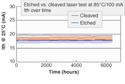
Cleaved laser facets defined by the crystalline planes of the epitaxial material are inherently perfectly smooth and vertical. Cleaved facets therefore provide ideal planar mirrors for the fabrication of FP edge-emitting lasers. To maintain the high facet quality needed for good FP laser performance, etched facets must meet stringent requirements for smoothness (root-mean-square surface roughness of approximately 20 nm) and verticality (90°± 2°) in the vicinity of the optical mode. When these requirements are met, performance of etched-facet lasers is as good as cleaved-facet lasers for the same epitaxial wafer material. For cleaved- or etched-facet lasers fabricated side-by-side on the same wafer, average threshold current is 18.0 ± 0.8 mA and 18.6 ± 0.4 mA, respectively (see Fig. 1). Threshold current over time also demonstrates equivalent stable aging behavior for lasers with both types of facet.In some semiconductor laser designs, performance can be enhanced through the use of non-normal facets that are angled or curved. Facet etching allows for the implementation of these designs, which can be used either alone or with an antireflection (AR) coating to reduce facet reflections in single-mode DFB lasers. Large angles introduce significant wavefront distortion penalties particularly as the critical angle for total internal reflection is approached. However, a standard AR coating reflectivity of -20 dB can be reduced by an additional 20 dB with a modest facet angle of just 6°. The resulting -40-dB reflectivity is difficult to achieve with AR coating alone on a normal-incidence cleaved facet. Besides angled facets, nonplanar or curved facets can serve as an integrated output lens, to improve the coupling efficiency from laser facet to external waveguide, for example.2 These types of laser-facet designs, which are not possible with cleaved facets, are readily attainable through etched-facet processes.
Increased flexibility to shorten the length of cavities is another benefit of etched facets that can be used to enhance performance. Because the cavity length of cleaved facets also equates to the chip length, such lasers must meet a minimum length determined by handling requirements. Cleaved-facet laser chips are typically 200 µm long or longer-anything smaller is problematic for handling. Etching facets allows for the decoupling of cavity length from chip size, thereby enabling significantly smaller cavities to be used which can be an advantage for laser speed and for controlling power requirements and heat dissipation in some designs.
Wafer-scale test
A primary advantage of etched-facet lasers is that the devices can be fully tested at the wafer level. An automated tester incorporating electrical and optical probes can screen devices on the wafer with high throughput. After testing is completed, an electronic wafer map is generated that allows good devices to be retrieved following die singulation.
Wafer-scale testing of etched-acet lasers at Xponent is done on an automated probe station manufactured by a commercial vendor that supplies testing stations to the chip industry. The probe station was adapted for full optoelectronic testing, incorporating standard electrical probes and proprietary “optical probes” to collect light emitted by the laser under test. The test system measures all DC laser characteristics including threshold current, threshold voltage, reverse leakage current, series resistance, linearity of the light versus current characteristics, peak wavelength, and other parameters. Total test time per device is less than 2.0 s, which includes 1.6 s to sweep the electrical input and process the data, and 0.2 s to mechanically step to the next device. The testing is normally performed with the laser wafer at room temperature, but the temperature-controlled wafer chuck allows testing at elevated temperatures if necessary.
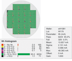
A typical wafer map displays threshold current for each laser in terms of color-coded bins (see Fig. 2). A histogram of the threshold current values and yield statistics can also be displayed. In addition to threshold current, a similar map can be generated for each measured laser parameter and all maps can be aggregated into a summary map that labels each laser as “pass” or “fail.” Passing lasers can also be binned in terms of performance level, if desired.In the future, to further increase wafer-test throughput, several enhancements to the automated probe testing station can be incorporated. Instead of testing lasers serially, for example, the addition of a modified probe head and duplicate optoelectronic test hardware would allow probe and test of multiple lasers in parallel. An automated wafer loader and machine-vision alignment system could also be added, enabling the probe testing station to process a cassette of laser wafers unattended.
Reliability
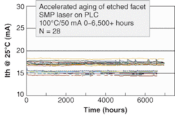
Any new manufacturing approach in optoelectronics must pass the hurdle of reliability before being accepted by the industry. Reliability data from 85°C/85% relative-humidity testing and accelerated lifetime testing of Xponent’s etched-facet Surface Mount Photonics(SMP) lasers show that devices are stable under very aggressive test conditions. In fact, adding a waveguide extension through the etched-facet process provides additional robustness by sealing the facet of the laser with dielectric making it impervious to moisture and less susceptible to galvanic corrosion.Accelerated lifetime testing of our etched-facet FP laser designed for an uncooled 2.5 Gbit/s transmission application indicates very stable laser performance over 6500 hours at accelerated conditions of 100°C heat-sink temperature with a high operating bias of 50 mA (maximum rated current; see Fig. 3). These accelerated results for 28 devices are equivalent to more than two million device-hours at typical 40°C operating temperature. We note that Xponent is not the only laser manufacturer capable of producing reliable etched-facet semiconductor lasers. BinOptics (Ithaca, NY) reports etched-facet lasers undergoing 12,000 hours of accelerated lifetime testing at 90°C with good reliability.
REFERENCES
1. A. Benzoni and T. Engelhard, Laser Focus World 40(6), S16 (June 2004).
2. D. W. Vernooy et al., Photonics Tech. Lett. 16(1) 269 (January 2004).
Al Benzoni is vice president engineering, Hank Blauvelt is chief technology officer, Mike Newkirk is a senior member of the technical staff, Joel Paslaski is a distinguished member of technical staff, and Rolf Wyss is technical manager for Xponent Photonics, 425 E. Huntington Drive, Monrovia, CA 91016-3632; e-mail: [email protected].


