MICROMECHANICS: Micromachines may solve lightwave network problems
Micromechanics may give lightwave systems designers the capability to build highly functional devices to keep up with the explosive growth in bandwidth.
David J. Bishop, Vladimir Aksyuk, Cristian Bolle, Randy Giles, and Flavio Pardo
The field of silicon-based micromechanics is just beginning to impact industries as diverse as automaking, aeronautics, cellular communications, chemistry, acoustics, display technologies, and lightwave systems. Research in this area over the last decade has produced microscopic versions of many macro machines. The technology continues to advance rapidly, driven by an estimated $200 billion annual market for very-large-scale integrated circuits and that industry's relentless development of related tools, techniques, and processes.
Ultimately, their size scale may make micromachines a particularly good match for solving optics problems, where the devices, structures, and relevant wavelengths range in size from one to several hundred microns. In lightwave systems, in particular, micromechanics may give systems designers the capability to build highly functional devices to keep up with the explosive growth in bandwidth.
FIGURE 1. This 1 x 2 MEMS optical switch can route light from the input fiber to one of two output fibers.
The fabrication method for silicon micromachines is similar to that for a silicon integrated circuit (IC). In a sequence of steps, materials such as polysilicon, silicon nitride, silicon dioxide, and gold are deposited and patterned on a silicon wafer to create a complex three-dimensional (3-D) structure. Unlike with an IC, though, the final step "releases" the device by etching away some material to leave sections free to move.
Although devices can be complex, fabrication costs could be relatively low with use of batch-processing techniques. Designers also have the flexibility to integrate micromechanical, analog, and digital microelectronic devices on the same chip to produce multifunctional integrated systems. The resulting microelectromechanical systems (MEMS) devices can be surprisingly robust and long-lived, especially those with parts that flex without microscopic wear points.
Lightwave system components
Potential lightwave network application areas include data modulators, variable attenuators, active remote nodes, active equalizers, add/drop multiplexers, optical switches (see Fig. 1), power limiters, choppers for power measurements, and optical crossconnects. The addressable market for these devices is huge, and several companies are aggressively pursuing it.
One such micromachine is a simple tilt mirror for use in a variable attenuator (see Fig. 2). The device consists of a mirror connected to a pivot point and an electrode. Apply a voltage to the electrode, and the plate rotates about the pivot and changes how light is reflected from an input optical fiber to an output fiber.
Once a system designer has built a single mirror, which can vary in complexity from a simple device to a multiaxis unit, it can be easy to fabricate many such devices at the same time on a wafer. Micro tilt mirror arrays also will work in an add/drop multiplexer for routing individual colors of light in a wavelength-division-multiplexing (WDM) system (see Fig. 3). In operation, each wavelength of light lands on its own mirror for routingeither to be carried on its way or dropped and detected at the node. Such functionality is normally hard to achieve without many costly components, each bought and assembled separately.
Optical switching
System designers can also build powerful micromachines to function as optical switches. One example consists of a polysilicon gold-plated mirror connected by a long arm to a parallel-plate actuator. It works like a child's seesaw, with the pivot point where the arm attaches to the plate. In the absence of an applied voltage, the gold mirror rests below the waveguide cores of two closely spaced fibers, and light transmits from one to the other with very little loss.
FIGURE 2. Micromirrors can range in complexity from a simple tilt mirror for a variable attenuator (above) to a complex micromirror, capable of two-axis rotation, that can route light in a range of directions to accomplish more-complex switching functions (below).
With a voltage applied between the actuator plate and the substrate, the electrostatic forces pull the plate down toward the substrate. The pivot forces the long arm off the substrate and lifts the gold mirror into the light path between the two fibers, which reflects light back down the fiber.
FIGURE 3. Batch processing techniques allow production of low-cost multiple devices on one wafer, such as this array developed for an add/drop multiplexer.
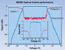
Two key attributes of the MEMS reflective switch are its thin silicon vanes and low-voltage electrostatic actuation (see Fig. 4). Thin shutters, comprised of a gold layer deposited on a polysilicon layer, are less than 2 µm thick and will fit into a very narrow gap between two optical fibers. Broadband, polarization-independent, fiber-to-fiber losses of less than 0.5 dB have been demonstrated in these MEMS switches with active fiber alignment. Researchers have achieved 0.8-dB loss with a "passive" assembly using guide rails to position the fibers. In addition to providing low insert loss, the narrow gap limits the optical spot size through the free-space region, enabling the switches to achieve extremely high contrast between the on and off stages, with a contrast ratio greater than 60 dB easily achievable. Clearly these devices can combine low insertion loss with very high contrast ratio. This high contrast is valuable because it eliminates unwanted signal feed-through that could otherwise lead to interference and crosstalk penalties.
The second attribute, electrostatic actuation, is ideally suited for low-power operation of these structures. Many applications only require the switch to change state infrequently. In these cases, the switch consumes energy to charge the capacitor plate, dissipating zero average electrical power. Even those situations with frequent reconfiguration require very little electrical power, typically less than several microwatts. This low power consumption is highly desirable in dense switch configurations. It also enables completely new functionality and applications, such as optically powered MEMS circuits.
In the future
The micromachines discussed above illustrate just a few ways that lightwave networks could benefit from the small size, scalability, low power consumption, and low fabrication cost of MEMS optical circuits. Rapid developments in optical MEMS technology are being driven by the immediacy of challenging optical network requirements. For example, now that rudimentary nonreconfigurable WDM optical add/drop multiplexers have been deployed in the field, the industry is fervently seeking to upgrade to devices that are fully reconfigurable.
FIGURE 4. To reduce production costs for this optical shutter fiber switch, designers incorporated self-assembly techniques that allow the hinged plate with the mirror to stand on its own during the release step. Chart below illustrates typical performance of a MEMS optical switch.
Optical switches based on MEMS can meet the functional requirements for these complex optical subsystems. In fact, they may provide the only practical solution when large numbers of add/drop channels are required.
Although no MEMS device has yet been deployed in an active lightwave network, the wealth of new capabilities presented by such optical devices makes them certain candidates for commercial success. The optical MEMS industry is expected to become a multibillion-dollar business in the next five years. Many companies identify MEMS as a strategic technology they cannot afford to neglect.
DAVID J. BISHOP, VLADIMIR AKSYUK, CRISTIAN BOLLE, RANDY GILES, and FLAVIO PARDO are researchers in the Micromechanics Research Department at Bell Labs, Lucent Technologies, 600 - 700 Mountain Hill, Murray Hill, NJ 07974; e-mail: [email protected].


