Electrons go ballistic in field-emission display
Incorporating news from O plus E magazine, Tokyo
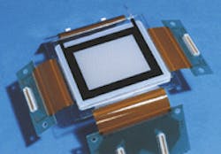
TOKYOResearchers at Matsushita Electric Works have joined with Nobuyoshi Koshida, a professor in the electrical engineering department at Tokyo University of Agriculture and Technology, to develop a display based on a novel electron emitter. The new ballistic electron surface-emitting display (BSD) is a type of field-emission display (FED) in which each pixel has an emission component that produces light by emitting electrons that strike a fluorescent body (see Fig. 1). Conventional FEDs use cone-shaped electrodes to emit electrons, but the BSD uses a different mechanism.
FIGURE 1. Screen of prototype multicolor BSD display is 2.6 in. (diagonal) with 53 x 40 pixels; each pixel contains red, green, and blue emission components. A gap of several millimeters between the electron-emission components and the fluorescent screen has no effect on image quality.
To produce the BSD, an electrode layer is first formed on a glass substrate, then a film of polysilicon is deposited. Clusters of microcrystals are formed within the film, and an oxide film tops the layer. A second electrode is then deposited.
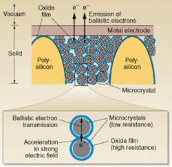
When a voltage is applied across the electrodes, the resulting electrons gain tremendous kinetic energy as they accelerate through the microcrystals. Electric resistance is high because of the oxide layer, meaning that the electrons are primarily accelerated within the oxidation film. The electrons move through the microcrystals with little dispersion, unlike ballistic electron transmission through regular solids. As a result, there is little energy loss. Also, all of the electrons are emitted in the same direction, perpendicular to the surface (see Fig. 2 on p. 52).
The BSD not only exhibits the qualities common to all active light displays, it also features low energy consumption compared to plasma displays. Matsushita estimates power requirements below 100 W for a 42-in.-diagonal panel. In addition, the structure of the BSD simplifies the manufacturing process. For example, because the electron beam does not spread, electron lenses typical of standard FEDs are unnecessary.
FIGURE 2. The emitter in a BSD relies on clusters of microcrystals and an oxide layer to coherently accelerate electrons toward a fluorescent screen. Inset shows acceleration mechanism.
Existing production lines for liquid-crystal displays can be used because the process of growing polysilicon films and electrodes on a substrate is the same as for liquid-crystal displays. Creating microcrystals from the polysilicon is a new process, but should not require significant adjustments.
Matsushita says that the BSD screens are readily scalable. Another benefit is that a BSD operates under low-vacuum conditions: although the space between the electron emitters and the fluorescent body must be a vacuum, it is not necessary to achieve the high-vacuum conditions required by conventional FEDs.
Matsushita has patented the electron-emitter technology, but because of its promise in the development of large-screen televisions and displays, the company is planning to widely license the technology to other firms.
Courtesy O plus E magazine, Tokyo


