PHOTONIC CRYSTALS: Intensity-dependent transmission protects sensors
Nonlinear absorption properties make photonic crystals useful optical limiters where protection is needed from sudden flashes of high-intensity light.
James S. Shirk and Armand Rosenberg
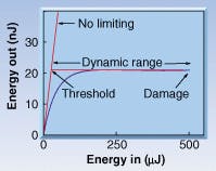
Optical limiters are devices that exhibit high transmission at normal light intensities and a transmission that decreases as the light intensity rises. This intensity-dependent transmission can keep the transmitted light energy below some maximum value. The devices can perform several useful optical functions, the most obvious of which is protecting optical elements and sensors, including the eyes, from damage by sudden flashes of high-intensity light. Desirable properties of a limiter include a low threshold, a fast response, and wide dynamic and transmission ranges (see Fig. 1).
FIGURE 1. Optical limiters are characterized by their dynamic range, threshold, and response time. A wide dynamic range, low threshold, and fast response time are desirable.
Limiters depend on a nonlinear optical process so materials that exhibit large nonlinearities are a critical part of these devices. Previously, limiters have usually relied on nonlinear absorption or refraction in an organic dye.1 More recently, nonlinear photonic crystals have been fabricated that incorporate these dyes, and these crystals can be used to make useful optical limiters.
Nonlinear absorption, where the sample absorbance increases with incident intensity, forms the basis of many current optical limiters. Changes in the index of refraction can also contribute to optical limiting. Nonlinear refraction, however, requires a method of converting the index changes into transmission changes. One way is to use the index changes to modify the focusing properties of a beam. A more-efficient option is to use photonic crystals.
Photonic crystals
Analogous to an ordinary crystal, a photonic crystal contains a highly ordered structure of unit cells. Whereas the structure of an ordinary crystal is defined by the atomic positions (lattice), the structure of a photonic crystal consists of a periodic modulation of the dielectric constant. In an ordinary crystal, the scale of the lattice periodicity is comparable to the electronic deBroglie wavelength; in a photonic crystal, the periodicity is comparable to the wavelength associated with a photon.
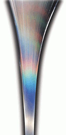
The periodicity of the dielectric constant modulation can be in one, two, or three dimensions, giving rise to corresponding 1-D, 2-D, or 3-D photonic crystals. Photonic crystals for the visible spectral region have a periodicity scale comparable to wavelength for visible light. Such crystals selectively reflect different wavelengths at different angles, so they are often strikingly beautiful materials (see photo, left). The gemstone opal is a naturally occurring example of a photonic crystal. Most, however, are artificially engineered to have certain desirable optical properties at specific wavelengths.
Light reflected off a drawn boule of nanochannel glass material shows the iridescence at different wavelengths that occur as the spacings of the glass structure vary.
On a practical level, these crystals can control the propagation of light, which leads to some important potential applications, including low-threshold lasers, waveguides, and optical limiters and switches. To construct a visible optical limiter or switch using photonic crystals, one must both construct a visible photonic crystal and devise a mechanism by which the crystal transmission responds to the incident-light intensity.
One useful method of producing 2-D visible photonic crystals is based on the nanochannel glass materials developed at NRL. Nanochannel glass consists of an ordered array, usually triangular, of holes or channels in a glass matrix
(see "Fabricating nanochannel glass" below). We have produced photonic crystals for the visible spectrum and described their optical properties over the past several years.2
Optical properties of photonic crystals
When a light beam passes through a photonic crystal, the modulation of the dielectric constant acts as a multidimensional diffraction grating, deflecting the rays in regular patterns. This is analogous to what is observed for x-rays passing through an ordinary crystal. The peaks in the diffraction pattern represent spectral regions where photons are unable to propagate through the photonic crystal (along certain directions) and are known as photonic stop bands or bandgaps. The spectral widths of these regions are determined by the symmetry of the crystal structure and they increase as the magnitude of the dielectric constant modulation increases. However, whereas for x-rays the effective modulation of the dielectric constant (arising from the atomic crystal lattice) is naturally very small, photonic crystals can be engineered with a much larger dielectric constant modulation. Consequently, the widths of photonic bandgaps can be engineered to be narrow or to cover a large spectral region.
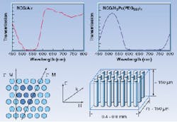
FIGURE 2. Photonic crystal based on nanochannel glass (NCG) in which the channels are filled with air has the transmission spectrum shown at left when measured along the high-symmetry G-M direction. In this case, a bandgap occurs between 510 and 560 nmthe reflectivity is high and the transmission can drop as low as 10-4. If the channels are filled with an index-matched phthalocyanine (Pc) dye, this bandgap disappears. The spectrum now shows only the dye absorption between 580 and 770 nm (right). Inset shows typical structure of a photonic crystal based on nanochannel glass.
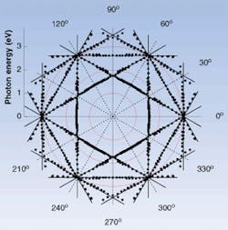
The characteristic optical property of a photonic crystal is the set of photonic bandgaps associated with it. The strengths and positions of the corresponding spectral features appearing in the transmitted or reflected spectra depend on the geometry and magnitude of the dielectric constant modulation (see Fig. 2). There is an intimate connection between the positions of the bandgaps and the underlying crystal structure (see Fig. 3).
Photonic crystal optical limiter
Fabrication of a photonic crystal optical limiter starts with the nanochannel glass structure. The channels are filled with a nonlinear material whose low-intensity refractive index matches that of the glass. Because there is no modulation of the refractive index, the photonic bandgap vanishes, and the transmission is high. When intense light is incident on the structure, the index of the nonlinear material is altered, a bandgap develops, and the transmission through the device drops (see Fig. 4). As shown in Figure 3, the energy of the first bandgap is not very sensitive to angle, so in appropriate directions the acceptance angle of such a limiter is relatively large.
FIGURE 3. Polar plot shows attenuation positions (photonic bandgap energies) observed in a 2-D photonic crystal with periodicity of 280 nm. Near the G-M direction (0° in this case), the energy of the first bandgap is not very sensitive to direction. This pattern of Brillouin zone boundaries is specific to the triangular lattice of the photonic crystal, a result reminiscent of x-ray analysis of the structure of ordinary crystals.
An effective nonlinear material is required to fill the channels in the nanochannel glass. The first photonic crystal limiter used a thermal change in the index of refraction.3 An absorber that efficiently converted the incident energy to heat was dissolved in a solvent for which the change in index with temperature is large. The index change after absorption was sufficient to cause the appearance of a substantial bandgap with incident fluences of a few hundred mJ/cm2. After a threshold is reached, the index modulation becomes large enough that the transmission of the photonic crystal switches off. This limiter is effective for pulses in the millisecond regime.
FIGURE 4. Nonlinear photonic crystal acts as an optical limiter by developing a photonic bandgap when subject to high-intensity light.
Better limiting can be achieved in a photonic crystal limiter by using additional nonlinear mechanisms. Recent studies of the optical properties of phthalocyanine (Pc) dyes at NRL have led to development of materials that combine a large nonlinear absorption with a large nonlinear refraction.4 In these materials, the nonlinear response includes excited-state absorption, excited-state nonlinear refraction, and thermal refraction. Some of these materials have been designed to be liquid or low-melting-point glasses so that they can be used to fill the tiny open channels in a nanochannel glass crystal.5 The resulting photonic crystals have large nonlinearities.
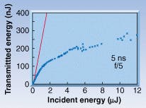
FIGURE 5. Curve shows optical limiting achieved by this Pc/NCG photonic crystal for short, 5-ns laser pulses. Transmitted energy is limited to just over 250 nJ.
The example in Figure 2 shows the spectrum of nanochannel glass filled with an index-matched Pc dyechosen to be chemically and physically compatible with the nanochannel glass (NCG) structure. This spectrum is identical to that of the Pc alone. The dye has a transmission window in the region where the photonic band gap of the air-filled crystal occurs. There is no bandgap in the index-matched crystal, but at high fluences the bandgap reappears, effectively blocking the transmission window. Improved limiting is observed at short times and for low fluences in this photonic crystal because the contributions from the nonlinear absorption and the photonic bandgap formation combine and their effects add (see Fig. 5). An additional advantage comes because the decrease in transmission is due in part to an increase in the reflectivity. The energy load on the nonlinear material is reduced, lowering the potential for damage to the material.
In summary, two-dimensional nonlinear photonic crystals can be fabricated by introducing nonlinear dyes into nanochannel glass structures. This gives photonic crystals where the modulation in the dielectric constant varies with the energy of the incident light pulses. The transmission of such photonic crystals varies rapidly with the incident-light intensity, which means they are promising as optical limiters. The Pc/NCG photonic crystals are more effective as optical limiters because changes in both the index of refraction and absorption contribute to limiting. The optical properties of these nonlinear photonic crystals can be engineered by a proper selection of the constituent materials and their ordering in the photonic crystal structure.
ACKNOWLEDGMENTS
The Office of Naval Research and the Naval Research Laboratory supported this work at NRL.
REFERENCES
- H. S. Nalwa and J. S. Shirk, in Phthalocyanines: Properties and Applications, C. C. Leznoff and A. B. P. Lever, eds., VCH Publishers (New York, 1996), vol. 4, p. 79.
- H.-B. Lin, R. J. Tonucci, and A. J. Campillo, Appl. Phys. Lett. 68, 2927 (1996); A. Rosenberg, R. J. Tonucci, and E. A. Bolden, Appl. Phys. Lett. 69, 2638 (1996).
- H.-B. Lin, R. J. Tonucci, and A. J. Campillo , Opt. Lett, 23, 94 (1998).
- J. S. Shirk et al., Appl. Phys. Lett. 63, 1880 (1993).
- A. W. Snow, J. S. Shirk, and R. G. S. Pong, J. Porphyrins and Phthalocyanines (submitted) and unpublished results.
JAMES S. SHIRK and ARMAND ROSENBERG are research scientists with the Optical Sciences Division, Naval Research Laboratory, Washington, DC 20375; e-mail: [email protected]; [email protected]. mil.
Fabricating nanochannel glass
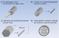
The first step in the fabrication of nanochannel glass-based photonic crystals consists of drawing, at elevated temperature, a glass rod inside a matching glass tube.1 The rod and tube are made up of different glasses, with the rod glass being acid etchable (a). The drawing process fuses the rod to the tube and produces thin composite filaments (b). These filaments are then stacked into a bundle, which is drawn again, fusing the filaments together and reducing the outside diameter to that of the initial filament (c). This process is repeated one more time by stacking sections of the first drawn bundle into a new bundle. The final composite glass material is cut into wafers and etched in acid (d). Each glass wafer contains an array of channels that can be filled with various optical materials. For the transmission experiments described in the main text, the wafers are oriented, ground, and polished to produce samples that have high-symmetry crystalline directions at normal incidence to the sample faces.
REFERENCE
- R. J. Tonucci, B. L. Justos, A. J. Campillo, and C. E. Ford, Science 258, 782 (1992).
