No one can ever have a printer that is too fast or has resolution that is too high. At least that is what many laser-printer manufacturers and researchers assume. In this pursuit of speed and print quality, laser scientists are now focusing their efforts on the lasers themselves, developing high-density laser-diode arrays to scan the entire width of a page without scanning mirrors and moving devices to shorter wavelengths to produce more dots per inch (dpi).
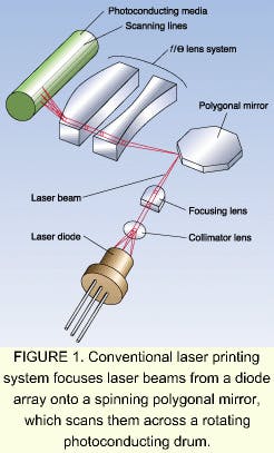
Conventional laser printers work by exposing a photoconducting material to laser light. For each pixel in the electronic image, a single dot of laser-exposed photoconductor is produced. In the areas where the photoconductor has been exposed, the device transfers toner to the output paper. The laser is scanned across the image line by line using a polygonal mirror that rotates at high speed (see Fig. 1).Such devices have long been the choice for high-end printing applications and have advanced through the years from 300 to nearly 1200 dpi, but this probably is not the performance ceiling. Even higher resolutions may be demanded to avoid the appearance of jaggedness in oblique lines and to allow for gray-scale and color reproduction.
To accurately reproduce color tones and shadings as well as textures with binary dots, a device requires far more dots per inch than the eye can resolve. Each time resolution doubles, the number of dots increases fourfold. To avoid diffraction effects, laser-beam size must increase as focused spot size decreases, increasing the size of the facets on polygonal mirrors. To maintain printing speed, the rotational speed of the polygonal mirrors must, therefore, be increased to produce more scan lines per second.
Eliminating the polygon
These speed gains place growing demands on the modulation of the laser diode necessary to generate crisply separated spots. A printing speed of two pages per second at 1200 dpi, for example, requires 200,000 scans per minute and a laser with a 400-MHz modulation frequency. Such high frequencies are extremely difficult to achieve in practice, and, as a result, higher resolution usually means lower printing speeds.
One option is to increase the number of simultaneous line scans by increasing the number of laser diodes. Ideally, if there are as many diodes as there are dots across a page, the polygonal mirror can be eliminated. Significantly higher printing speeds would then be possible without increasing the modulation frequency fed to each diode. To provide printing speeds approaching 1200 dpi requires arrays of thousands of diodes and very close packing.
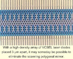
At Xerox (Palo Alto, CA), Christopher Chua and colleagues are attempting to reach this ambitious goal using densely packed surface-emitting laser diodes spaced only 3 µm apart on a gallium arsenide (GaAs) wafer.1 With such close spacing, the resulting printers are compact, allowing more chips per wafer. There also is less probability that a given printer will contain lasers lying on wafer defects, so manufacturing yield should increase.
While light-emitting-diode (LED) printers have been on the market for some time, the higher overall efficiency of laser diodes allows far-denser packing because less heat is produced. In addition, vertical-cavity surface-emitting lasers (VCSELs) have a tighter beam than edge-emitting lasers and can deliver roughly ten times more light for a given input power than LEDs.
Since densely packed VCSEL arrays require high efficiency to avoid overheating, the Xerox researchers developed a design that was oxidized laterally to facilitate power conversion. They also re-examined the array architecture. The reason lies with the selectively oxidized aluminum gallium arsenide (AlGaAs) layer, which is placed near the active region of the conventional architecture to funnel current into the optical mode. This layer is created by etching a pillar through the top distributed-Bragg-reflector material to reach the oxidation layer. Then the layer is laterally oxidized inward from the sides of the etched mesas. However, the mesas produce a highly uneven wafer surface, which makes it difficult to route electrical contacts in a very dense array.
To resolve this issue, Chua and his team replaced the mesa etch with sets of small via holes. The holes serve the same purpose of exposing the buried oxidation layer, but they leave an intact wafer surface for electrical routing. Holes are arranged along the corners of a hexagon so that the oxidation fronts from the holes expand and merge to enclose a laser aperture at the center of the hexagon.
The research team has demonstrated the array technology with a pitch of only 3 µm and an array of 200 individual lasers (see photo on p. 143). Ultimately, it may be possible to scale the architecture to produce even longer arrays, limited only by issues of wafer size and yield. This, in turn, may make it possible to produce a single bar covering the entire page width using several thousand lasers.
Shorter wavelengths, smaller dots
In the quest for better resolution, one obvious route for manufacturers is to reduce the wavelength of light used by the laser printer. Since the conventional AlGaAs system produces 780-nm output, the next step is to go to aluminum gallium indium phosphide (AlGaAsP) systems that provide 630-nm light. With this design, however, comes increasing difficulty in fabricating the refractive-index guide structure that produces the separate laser beams.
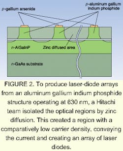
Recent work by Shin'ichi Nakatsuka and Susumu Saito at the Central and Katsuta Research Labs of Hitachi Ltd. (Tokyo and Ibaraki, Japan) presents a possible way around these difficulties.2 Their idea is to form the diode-array elements by diffusing zinc in an alternating pattern into the system. This creates a region with a comparatively low carrier density, conveying the current and creating an array of laser diodes (see Fig. 2).The Hitachi team reports that its laser diode performed relatively well and had a threshold current density close to that of conventional diode arrays, as well as one-third of the cavity loss. With the eventual commercialization of devices such as these, end users should expect to see faster, more-efficient laser printers in the next few years.
REFERENCES
- C. L. Chua et al., Proc. SPIE 3626,.87 (June 1999).
- S. Nakatsuka and S. Saito, Proc. SPIE 3628, 196 (June 1999).
About the Author
Eric J. Lerner
Contributing Editor, Laser Focus World
Eric J. Lerner is a contributing editor for Laser Focus World.


