Engineered artificial graphene in semiconductors: Beyond natural graphene
Columbia University (New York, NY) engineers, working in partnership with Princeton University (Princeton, NJ), Purdue University (West Lafayette, IN), and Istituto Italiano di Tecnologia (Genova, Italy), have engineered “artificial graphene” by recreating its structure in a semiconductor quantum-well device. Compared to the fixed position of atoms in natural graphene, the artificial graphene can be engineered with different atomic spacings and lattice configurations, making it highly versatile for condensed-matter research and other areas of optoelectronics that hold promise for graphene materials, including information processing and novel semiconductor switches and transistors.
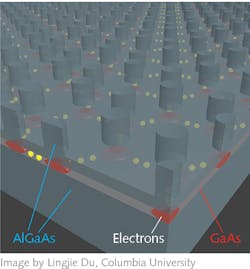
To fabricate the artificial graphene, available state-of-the-art semiconductor processes were used to create layers of aluminum gallium arsenide (AlGaAs) and GaAs that comprised a quantum well over which a hexagonal array of quantum dots was contained beneath nanopillars created in the top layer of the electron-confining structure. These hexagonal patterned GaAs structures—which behave like artificial atoms only 50 nm apart—allow quantum-mechanical interactions much like the electron-sharing behavior of atoms in a solid. The nanofabrication processes used enable engineering of novel structures that can be used to manipulate the flow of electrons and photons to mimic not only graphene’s myriad uses, but to define new structures with advanced capabilities still being imagined. Reference: S. Wang et al., Nature Nanotechnol., 13, 1, 29–33 (2018).
About the Author

Gail Overton
Gail Overton served as a senior editor for Laser Focus World from 2004 through 2020. She has more than 30 years of engineering, marketing, product management, and editorial experience in the photonics and optical communications industry. Before joining the staff at Laser Focus World, she held many product management and product marketing roles in the fiber-optics industry, most notably at Hughes (El Segundo, CA), GTE Labs (Waltham, MA), Corning (Corning, NY), Photon Kinetics (Beaverton, OR), and Newport Corporation (Irvine, CA). During her marketing career, Gail published articles in WDM Solutions and Sensors magazine and traveled internationally to conduct product and sales training. Gail received her BS degree in physics, with an emphasis in optics, from San Diego State University in San Diego, CA in May 1986.