OPTICAL SENSORS: Nanoscale microcavity detects single particles
One-dimensional photonic crystals and photonic-crystal microcavities have already been used for the detection of DNA, proteins, and even bacteria. Photonic-crystal platforms are excellent for biosensing as the sample does not require staining with fluorescent or radioactive tags. Taking this technology one step further, researchers at the University of Rochester (Rochester, NY) have developed a two-dimensional (2-D) photonic-crystal sensor with a central defect that can detect single particles with diameters on the order of 50 nm (hepatitis virus) and 100 nm (influenza A virus).1
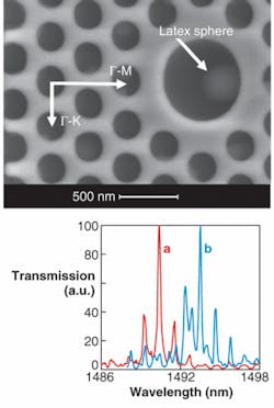
To achieve single-particle detection, the targeted particle must be guided into the defect area within the photonic-crystal microcavity. The photonic-crystal structure is fabricated using electron-beam lithography on a silicon-on-insulator (SOI) wafer with a silicon lab thickness of 400 nm. A hexagonal array with a lattice constant of 400 nm and a pore diameter of 240 nm surround a central defect-a center hole with a diameter of 685 nm. These parameters were selected so that the resonant wavelength falls within the tuning range of the 1440 to 1590 nm tunable laser used in the experiments.
A focused, TE-polarized beam is input to the 2-D waveguide by a tapered, lensed polarization-maintaining fiber. The transmitted signal is coupled out in like fashion and measured with an indium gallium arsenide (InGaAs) detector with a nitrogen cooling system to remove thermal noise. Alignment and monitoring of radiation losses is accomplished with an infrared camera.
By designing the 2-D photonic-crystal waveguide to have a central defect hole approximately three times larger than the surrounding holey matrix, particles with diameters on the order of the central defect can be trapped inside the defect while other particles can ride on top of the surrounding hole matrix without disturbing the measured spectral shift. When a particle is trapped inside the central defect, small refractive-index changes inside the defect hole cause a change in the spectral response of the device.
To demonstrate device operation, a latex sphere with a diameter of 370 nm and a refractive index of around 1.45 is captured inside the microcavity defect (see figure). Comparison of the spectral signature before capture and after capture shows a pronounced red shift of approximately 4 nm. It was also determined that the position of the sphere inside the cavity influences the redshift value as well.
Because this technique can detect single particles with diameters less than or equal to 50 nm, it should also be able to detect SARS and H5N1 bird flu. Although delivery of these particles to the central defect is challenging, membrane filters or microfluidics channels could be incorporated in the device to improve particle capture.
“We decided to use photonic crystal on SOI as the platform because of the small device footprint, the ease of on-chip integration with other photonic components, and the potential of mass production,” says Mindy Lee, researcher and Ph.D. candidate. “Our first step was to demonstrate that the sensor has sensitivity at a single biomolecule level. However, our ultimate objective is to provide label-free solutions for research in pharmaceutical industry, clinical diagnostics, and biosecurity.”
REFERENCE
1. M.R. Lee and P.M. Fauchet, Optics Lett.32(22) 3284 (Nov. 15, 2007).
About the Author

Gail Overton
Senior Editor (2004-2020)
Gail has more than 30 years of engineering, marketing, product management, and editorial experience in the photonics and optical communications industry. Before joining the staff at Laser Focus World in 2004, she held many product management and product marketing roles in the fiber-optics industry, most notably at Hughes (El Segundo, CA), GTE Labs (Waltham, MA), Corning (Corning, NY), Photon Kinetics (Beaverton, OR), and Newport Corporation (Irvine, CA). During her marketing career, Gail published articles in WDM Solutions and Sensors magazine and traveled internationally to conduct product and sales training. Gail received her BS degree in physics, with an emphasis in optics, from San Diego State University in San Diego, CA in May 1986.
