OPTOELECTRONIC APPLICATIONS: NANOPHOTONICS - Silicon photonics sets the stage for optical datacom
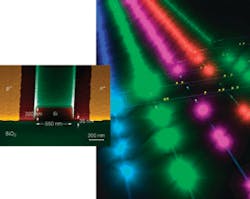
Last December, researchers from IBM T. J. Watson Research Center (Yorktown Heights, NY) announced another breakthrough in their quest to build a supercomputer-on-a-chip: the ability to transfer data between processor cores on a single chip 100 times faster than ever before by using photonics rather than electronics.1 According to the company, its new silicon Mach-Zehnder electro-optic modulator is 100 to 1000 times smaller than previously demonstrated modulators of its kind, paving the way for all-optical routing networks to one day be integrated onto a single chip (see Fig. 1).
This device is the latest advance to come out of IBM’s silicon nanophotonics program; in 2006 the company demonstrated ultracompact optical buffers with ring resonators on a silicon chip, and last March at the 2007 Optical Fiber Conference (Anaheim, CA), IBM researchers unveiled a 160 Gbit/s, 16-channel CMOS optical transceiver that they had coupled with other optical components made in more-exotic materials such as indium phosphide (InP) and gallium arsenide into a single, integrated package just 3.25 × 5.25 mm in size.2“Work is under way to pack many more computing cores on a single chip, but today’s on-chip communications technology would overheat and be far too slow to handle that increase in workload,” said T. C. Chen, vice president of science and technology at IBM Research. “What we have done is a significant step toward building a vastly smaller and more power-efficient way to connect those cores, in a way that nobody has done before.”
The key, according to IBM, Intel, and other companies and research groups around the globe, is silicon. Today’s commercially available optical modulators are typically based on lithium niobate and III-V compound semiconductors. But with its high refractive index, thermal conductivity, and optical-damage threshold, plus excellent linear and nonlinear optical properties (especially in the mid-infrared region), silicon presents a very attractive platform for ultracompact photonic devices.3 It is transparent at the wavelengths already used in telecom—from 1200 to 1700 nm—and transmits photons across a chip very well at these wavelengths. In addition, by adopting a substrate material that is CMOS-compatible, decades of materials and process knowledge can be leveraged during fabrication, eventually enabling high-volume production of silicon photonic devices.
“There is a lot of interest in silicon being one of the main technologies that could continue to allow for scaling computer performance,” says Will Green, lead scientist in silicon photonics at IBM. “We are trying to develop a low-power, high-bandwidth communication technology for the chip, not make a completely optical computer. We want to use optics where it makes the most sense for the interconnects, both for inside the computer or as a compact on-scale interconnect for communicating between multiple cores. A chip that could do on- and off-chip communications with an optical layer that allows the data to be transmitted.”
Competition in silicon photonics has intensified in recent years, with players in both academia and industry aggressively working to achieve completely integrated CMOS photonics. In mid-2007, researchers at Intel announced that they had demonstrated the world’s first 40 Gbit silicon laser modulator based on a Mach-Zehnder interferometer, with the ability to encode optical data at 40 billion bits/s. This breakthrough followed a series of technology “firsts” in silicon photonics from Intel: in 2004, the demonstration of a silicon-based optical modulator with bandwidth in excess of 1 GHz; in 2005, the demonstration of data transmission at 10 Gbit/s using a silicon modulator; and in 2006, in collaboration with John Bowers of the University of California, Santa Barbara, the first electrically pumped hybrid silicon laser that successfully integrates the light-emitting capabilities of InP with the light-routing and cost advantages of silicon (see www.laserfocusworld.com/articles/304010).
“The exciting piece is that before, if you wanted to do nanophotonics in the III-V world, we didn’t have the ability to process these devices,” says Mario Paniccia, director of Intel’s Photonics Technology Lab (Santa Clara, CA). “But we now have the ability to build photonic devices in silicon with the same manufacturing processes we already use, and to be able to scale this over time in terms of size and cost.”
Nano or not?
In fact, while most of the silicon photonic components are not yet of “official” nanoscale size, many of the critical processes used to create them are. At IBM, for example, the phrase “silicon nanophotonics” applies not just to the bits and pieces that are assembled on a chip but to the fabrication of those bits and pieces. IBM researchers have been able to shrink their silicon waveguides down to 500 nm wide by 200 nm tall; while these are not nanoscale dimensions along the lines of, say, carbon nanotubes, they do require very precise manipulations on the nanoscale to make them function optimally.
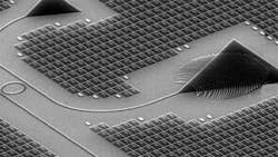
For example, using a standard CMOS line, IBM has patterned silicon photonic devices on 200 mm SOI wafers with 220 nm of lightly p-doped Si. A 50-nm-thick oxide was deposited on the wafers via low-pressure chemical-vapor deposition. The waveguides and silicon taper of the fiber coupler were defined in one step by electron-beam lithography, and the photonic-crystal patterns were routinely overexposed to smooth out the effects of fracturing circles into polygons for pattern writing. Three lithography steps followed, one to transfer the resist pattern to the oxide hard mask, the next to mask the strip waveguides and coupler regions to protect them from being underetched, and the third to define the epoxy polymer for the fiber coupler.
“The ‘nano’ part of this is about needing to control the performance on the nanoscale, such as scattering,” Green says. “An integral part of designing our devices to work properly involves controlling their dimensions to nanometer-scale lengths. The surfaces of these devices need to be smooth on the scale of a few nanometers, and you need to control the device dimensions to the order of a few nanometers or performance will shift from what you designed. We are able to scale devices to very small scale on a chip, but we also need to ensure that the manufacturing processes allow for those kinds of tolerances.”
Kotura (Monterey Park, CA), which claims to be the only company currently shipping a commercial silicon-photonics component, is also focused on implementing nanoscale fabrication techniques for its eight-channel variable optical attenuator (VOA), which is used for automatic channel equalization in add/drop multiplexers in metro area networks. Kotura’s primary focus is on silicon-photonics devices and processes to enable 100 Gbit Ethernet networks, using silicon as the substrate for both the lasers and the detectors and as the mux and demux of the wavelengths.
“When you are in the semiconductor world and you say ‘nanophotonics,’ you are referring to the lithography,” says Arlon Martin, vice president of sales and marketing at Kotura. “Just because you have very small lithography it doesn’t mean that the pads and the chips are nano. We use nanoscale processes and standard lithography equipment not just to make smaller waveguides but to achieve very smooth surfaces and sidewalls on the waveguides. We’ve developed techniques for getting very smooth sidewalls by utilizing the interplay between etching processes and lithography.”“If you look at one of our transceivers today, it is kind a big box, but if you take apart the box, the transceiver itself is really just a couple of square millimeters in size, and we think we can shrink this down with the same functionality to a couple of hundred square microns,” says Cary Gunn, founder and CTO of Luxtera. “The reason everyone is interested in silicon photonics is not because you are able to do something you can’t already do, but because you can do it much more cost-effectively and with greater functionality using existing mass manufacturing techniques and processes with resolutions at the single nanometer scale. For long-wavelength light, the diffractive limit is around 150 nm, and it took the manufacturing processes to get below that limit before we could really begin to make these parts.”
Toward the silicon laser
While each of these advances has been important to the development of all-silicon photonic ICs, the “holy grail” remains the silicon laser. Current silicon-photonic chips utilize an external laser source coupled to the chip via an optical fiber or flip-chip bonding, but there is great interest in having the light source on the chip itself.
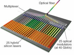
The Intel/UCSB hybrid silicon laser is a step in this direction. It utilizes an InP-based material bonded directly to a silicon waveguide. The key to manufacturing the device is the use of a low-temperature, oxygen plasma to create a thin oxide layer (roughly 25 atoms thick) on the surfaces of both materials. When heated and pressed together, the oxide layer functions as “glass glue,” fusing the two materials into a single chip. When voltage is applied, light generated in the InP-based material passes through the oxide “glue” layer and into the silicon chip’s waveguide, where it is contained and controlled, creating a hybrid silicon laser. The first hybrid silicon laser was about 800 µm long, but future generations will be “significantly smaller,” says Intel. Beyond that is the all-silicon laser, which is still some years away.
“The hybrid silicon laser is exciting, but I think we are a long way away from having a pure silicon laser,” Paniccia says. “Still, you want to end up with all silicon because while the hybrid laser is the best of all worlds it is not the ‘holy grail’ because you are still buying or growing the indium phosphide and that is not cheap. The point of the silicon laser is that the entire device can be processed in silicon, which would further reduce costs.”
REFERENCES
1. W.M.J. Green et al., Optics Express 15 (2007).
2. F. Xia, L. Sekaric, Y. Vlasov. Nature Photonics 1, 65 (2006).
3. B. Jalali, S. Fathpour, J. Lightwave Tech. 24, 12 (2006).
About the Author
Kathy Kincade
Contributing Editor
Kathy Kincade is the founding editor of BioOptics World and a veteran reporter on optical technologies for biomedicine. She also served as the editor-in-chief of DrBicuspid.com, a web portal for dental professionals.


