MICRO-OPTICS: Laser writing advances micro-optics fabrication
TASSO R. M. SALES AND G. MICHAEL MORRIS
Micro-optical manufacturing techniques have enjoyed remarkable progress in the last few years, transitioning from unique custom components for highly specialized applications to large-scale mass production for consumer products. At the core of this evolution are precision micro-optics solutions that provide high-performance light-control capabilities with robust design structures suitable for volume manufacturing. State-of-the-art lithographic analog micro-optics fabrication techniques create microlens arrays, beam shapers, and diffusers for a myriad of applications in laser and solid-state lighting control.
From binary to multilevel and analog
Behind the evolutionary track of micro-optical components from niche to consumer applications is the increased capability to manufacture components with improved surface accuracy, as well as the development of robust design structures for a variety of applications. During the late 1980s when micro-optics started to gain attention as viable technology, the field quickly branched from the original binary optics approach to produce microelements along two distinct avenues: multilevel and analog components. Researchers quickly realized that, to achieve optimum performance, surface structures had to be implemented as continuous-relief profiles. Initially, however, there was no way to produce the required continuous surface profiles and the solution was to approximate the continuous surface profiles by a multilevel staircase profile.
A well-known and particularly educational example of the multilevel approach consists of approximating the continuous profile of a diffractive lens with a staircase of N levels. It can be shown that the lens efficiency, or fraction of the input energy concentrated at its focal point, depends on N as sinc2(1/N), where sincx represents the function sinπx/πx. As N increases, the efficiency also increases as the multilevel approximation more closely resembles the continuous lens.
The multilevel approach to micro-optics requires alignment and exposure of multiple masks and, in practice, the total number of masks is generally four or fewer, implying a maximum of 16 levels (the number of distinct levels depends on the number of masks M as 2M). Accordingly, a 16-level multilevel lens is approximately 98.7% efficient, indicating that for many applications, four masks can be quite enough.
Although performance close to that of the ideal surface profile can be achieved with the multilevel approximation, this method is most suitable for thin structures such as diffractive elements, whose depth is on the order of the wavelength of light, and as long as feature sizes allow sufficiently accurate alignment of the various masks. Although multilevel fabrication has achieved a high level of sophistication, the limitation to thin structures and relatively large features restricts its applicability to specialized applications.
Grayscale masks
Even as multilevel fabrication developed, it became clear that ultimately, continuous surface structures would be required if micro-optical elements were to find widespread applicability. An approach that emerged somewhat naturally from lithographic mask exposure processes uses so-called “grayscale” masks in which a photosensitive material is exposed through a mask with variable transmission, as opposed to the usual binary photomasks. The grayscale mask process is based on contact exposure but requires a single step to produce an analog surface pattern. Not unexpectedly, grayscale masks are more expensive than simple binary masks, but their use is justifiable in applications in which the use of multilevel profiles is difficult or even undesirable, such as microlens arrays.
Similar to multilevel components, micro-optics based on grayscale technology are commercially available. However, because grayscale micro-optics rely on contact exposure, the types of patterns that can be produced are limited, particularly with respect to depth and slope angles.
Laser writing
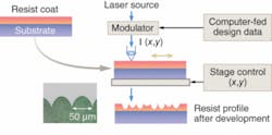
Another approach for producing precision analog micro-optics utilizes a single-point laser exposure of a photosensitive resist, or laser writing. In laser writing, the tool is a focused laser spot that is modulated as it scans the surface of a resist-coated substrate. When using resist, a high exposure dosage implies more material removal upon development, while a lower dosage means less material removal. A key difference from a machining process, such as single-point diamond-turning, is that there is no mechanical contact with the resist and there are no limitations on the types of pattern that can be produced.
Diamond turning, and more generally machining, is typically limited to rotationally symmetric or relatively simple surface profiles, although there has been recent progress using so-called “fast-tool servo systems,” in which machining allows the production of fairly general components with asymmetric profiles. However, there are more-complicated patterns such as diffusers that require a large number of microstructures to be produced with little symmetry-an impractical, if not impossible, task for machining, but an easy task for laser writing.
The basic steps involved in single-point laser writing begin with a substrate made of any sufficiently flat material, but generally glass or silicon (see Fig. 1). After an initial cleaning step, the substrate is coated with a uniform layer of photosensitive resist with a thickness that depends on the nature of the micro-optic to be produced (typically around 100 µm or less).
There is a continuous push in the industry to produce thicker uniform coatings because there are many products that require deep resist processing. Microlens arrays are a prime example: an f/1 lens with a diameter of 250 µm has maximum sag of about 63 µm. As the diameter increases so does the depth, and there are many applications that require microlenses with diameters of several millimeters. Although it is possible to produce micro-optical elements with depth beyond that of the resist coating thickness using complementary technologies such as reactive-ion etching, for instance, this approach is more time-consuming and expensive.
Optimizing laser-writing parameters
In the laser-writing process, two parameters are of fundamental importance for the laser beam producing the pattern: beam size and raster spacing (distance between two consecutive scan lines). The beam size has a direct relation to the feature sizes that can be produced, while the raster spacing affects surface roughness.
As a general rule, the beam size should be several times larger than the raster spacing to ensure surface smoothness. The exact relationship between beam size and raster spacing, however, is not strict and other considerations need to be taken into account such as the purpose of the micro-optic (imaging or nonimaging applications), wavelength of operation (ultraviolet, visible, or infrared), as well as more practical concerns such as the time needed to scan the substrate and which post-processing operations are necessary (etching, replication, and electroforming).
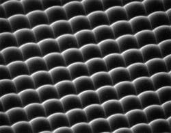
As a first approximation, a surface structure produced by laser writing can be described as the convolution between the target surface and the writing beam, which leads to some distortion of the design pattern, particularly at sharp corners. Similarly, vertical sidewalls are spread by an amount on the order of the beam size. For analog structures that require smooth surfaces, the beam size is usually fairly large, making the laser-writing process not adequate for patterns that require steep transitions such as in diffractive or Fresnel lenses (although the presence of steep transitions on random diffuser patterns are less of a concern). The finite beam size, however, does not preclude the production of high-fill-factor lens arrays (see Fig. 2). In fact, microlens arrays with 100% fill factor and controlled profile can be readily produced.The exposure process for laser writing takes place in a single step that corresponds to a full scan of the pattern area. This is usually the longest part of the process and-depending on the speed of the stages, raster spacing, and pattern size-can take from a few minutes to several days. Following exposure, the resist is developed to reveal the written pattern.
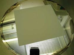
The resist master is a fragile material that requires storage in a controlled environment to prevent deterioration and/or damage. For this reason, other techniques have been developed to transfer the resist pattern into more durable or easily reproducible materials. Some of these techniques include polymer replication, reactive-ion etching, and electroplating. Polymer replication enables the creation of several submasters from the initial resist master and from these submasters the creation of products. Etching enables the transfer of the resist pattern into a durable, hard substrate such as fused silica. The glass master can then be used to produce other polymer submasters and so on. With electroplating, the resist master is turned into a durable metal master-particularly useful in the production of polymer products in the form of injection-molded plastic or films (see Fig. 3).Applications
Since the early days of binary optics, fabrication capabilities have evolved significantly to a point where micro-optical elements have become integral to a great number of applications in specialized and in consumer products.
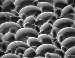
Perhaps the most well-known examples of micro-optical elements are diffusers and microlens arrays. Diffusers, in particular, have undergone remarkable progress in performance, thanks to innovative design forms that rely on assemblies of microlens units (see Fig. 4). Until very recently commercially available diffusers were limited to Gaussian intensity profiles, basically the same type of scatter seen from ground glass.Thanks to developments in micro-optics fabrication techniques, diffusers are no longer mere light homogenizers but efficient beam shapers that spread light in a controlled fashion both in energy distribution and intensity profile. These diffusers depart from other technologies in that light control is achieved by selective production of local slopes according to specific design rules that define both local and global properties of the diffuser. This type of sophisticated micro-optic component requires a fabrication technique that can address a pattern area on a point-by-point basis and is also able to handle large amounts of data, making the laser-writing approach particularly suitable.
TASSO R. M. SALES is vice president for product development and G. MICHAEL MORRIS is CEO of RPC Photonics, 330 Clay Road, Rochester, NY 14623; e-mail: [email protected]; www.rpcphotonics.com.


