Newsbreaks
Photopatterned sol-gel optical sensors measure oxygen concentration
Sol-gel materials are being fashioned into chemical sensors by researchers at Dublin City University (Dublin, Ireland). They have developed an ultraviolet photopatterning technique to fabricate ridge waveguides and spot arrays of an inorganic-organic sol-gel doped with an oxygen-sensitive ruthenium complex. The sensor detects the gas by meas-uring oxygen-quenching of the luminescence emitted by the ruthenium complex when excited by blue light.
The chosen sol-gel material has been previously used to produce integrated optical components for telecommunications applications. By varying the pH of the sol and the water:precursor ratio, the porosity and structure of the sol-gel can be varied, with high porosity essential to the chemical sensor's function. Contact lithography and subsequent rinsing by a solvent produced 14.5-µm-thick waveguides or spot arrays. Excited by 450-nm light from a light-emitting diode, sensors fabricated at different pHs were tested in a gas-flow cell. The sensitivity depended almost linearly on the pH of the initial sol. Pore size can be tuned for various sensing applications. Uses include sensor arrays, micro-total-analysis systems, and integrated optical sensors. Contact Brian MacCraith at [email protected].
Dual-material photonic crystal contains quantum-well light emitters
Photonic crystals (PCs) containing light emitters can potentially tailor the emitters' spectral and directional output. Integrating emitters into PCs is not an easy task, though. Researchers at Kyoto University are creating PCs of alternating layers of indium phosphide (InP)-based light emitters and gallium arsenide (GaAs) structures—two very dissimilar materials. The light emitter is a quantum well and the GaAs provides a foundation with an easy-to-control surface state. A layer is aligned to the one below it with a laser-diffraction alignment technique; after contact, the two layers are fused at temperatures of up to 525°C. An InP substrate supporting the light emitter is etched away, clearing the way for the next layer.
The researchers conducted a careful analysis of thermal stress under fusing induced by the different thermal-expansion coefficients. They found both theoretically and experimentally that the induced strain is greatest at the wafer's edge, causing debonding at temperatures ranging from 220°C to 300°C. The preferred method of fabrication was to thin the InP substrate to 150 µm so that it could stretch with the GaAs, and fuse the layers at a temperature of no greater than 300°C. Contact Shinpei Ogawa at [email protected].
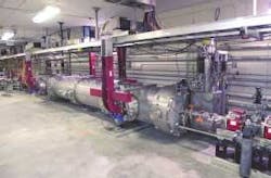
Aiming at 10 kW, infrared free-electron laser achieves first light
The dismantled free-electron laser (FEL) at the Department of Energy's Thomas Jefferson National Accelerator Facility (Jefferson Lab; Newport News, VA), which in 1999 produced 2.1 kW of infrared light, is being replaced by an upgraded version that is slated to produce 10 kW of infrared and 1 kW of ultraviolet light. Jefferson Lab researchers have now achieved "first light" in the upgraded version. The emission was tunable from 5.8 to 6.3 µm and reached a peak power of 200 W at 5.85 µm during a 200-µs pulse. The output was limited in power by the low current in the first experiment.

All photon optics are now cooled and have lower losses; electron-beam optics can handle higher energy. Active optics will maintain laser mode characteristics over a large power range. The ultraviolet laser will use cryogenic sapphire mirrors. Shown here, the FEL's new cryomodule (a superconducting magnet through which the electron beam is accelerated) operates with 80 MV of acceleration and may reach 100 MV per module. Aided by installation of the last energy-recovery magnets, the FEL is slated to reach its 10 kW average power by summer's end. Contact Stephen Benson at [email protected].
Liquid-crystal lens focuses electrically
A lens that is focused electrically instead of by mechanical motion would result in simple and rugged lens assemblies. Engineers at CRL Opto (Fife, Scotland) have developed a version of this sort of lens that relies on liquid crystal for tunability. The prototype liquid-crystal variable lens is based on an approach developed at the University of Durham (Durham, England) called modal addressing, in which the spatial phase properties of the lens are smoothly controlled without the requirement of a pixelated structure.
A standard nematic cell contains modified planar electrodes that control the spatial distribution of the electric field within the lens. Control electronics vary the amplitude and frequency of the drive signal to vary the refractive-index profile in the liquid crystal. The prototype has a 5-mm aperture and a focal range of from 500 mm to infinity. The lens has a short-wavelength cutoff of 400 nm and a switching speed of 1 s. The engineers can build cylindrical versions as well as lenses with larger apertures, but note that larger-diameter lenses are proportionally larger in minimum focal length as well. Contact Ruppel Joshi at [email protected].
Fluidic lens focuses by pressure
In another version of a lens focused in a nonstandard way, researchers at the University of California, San Diego (La Jolla, CA) have fabricated fluidic adaptive lenses in which fluid is forced between a membrane and a rigid transparent substrate to vary focal length. A syringe controls the fluid displacement. The researchers were inspired by living creatures' eye lenses, which are deformed by muscles to change focus.
A polydimethylsiloxane (PDMS) lens chamber is bounded by a glass slide and a PDMS membrane; both PDMS structures were formed by soft lithography and then attached together using oxygen plasma bonding. The 20-mm-diameter lens deforms elastically when under fluidic pressure. Focal length ranged from 41 to 172 mm at pressures ranging from 5865 to 400 Pa; resolutions at the two extremes were 12.7 and 8.98 lp/mm. The lens reaches its highest resolution of 25.39 lp/mm at a 62-mm focal length. The numerical aperture of the lens at its shortest focal length is 0.24, similar to that of the human eye with pupil at its most wide open. Contact De-Ying Zhang at [email protected].
Gallium nitride becomes new periodically poled nonlinear crystal
Researchers at Lucent Technologies' Bell Laboratories have demonstrated second-harmonic generation in periodically poled gallium nitride (PPGaN) by first-order quasi-phase-matching. The material has a transparency window of 365 nm to 13.6 µm, a range much larger than the competing materials of lithium niobate and gallium arsenide. The transparency window can be extended deeper into the ultraviolet by replacing GaN with AlxGa1-xN. Such a large transparency window will allow wavelengths to be generated by sum- or difference-frequency generation in the far infrared and near ultraviolet with potential applications in nonlinear optical devices for telecommunications as well as nonlinear light sources for biochemical detection in the far infrared and deep ultraviolet.
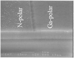
In contrast to lithium niobate, which is electric-field-poled, PPGaN is poled during fabrication by plasma-assisted molecular-beam epitaxy. A polarity-patterned GaN template is generated by growth of an aluminum nitride buffer layer followed by lithography, etching, and then thick regrowth that produces the Ga- and N-polar regions (seen in this scanning-electron micrograph). The 4-µm-thick PPGaN with 17.2-µm periodicity was cut into a 1.2-cm-long sample and the end facets were mechanically polished. Light from a femtosecond laser with a 1658.6-nm wavelength and 7-mW average power was converted into 9 µW of second-harmonic power, for a normalized conversion efficiency of 12.76% W-1cm-2. Contact Aref Chowdhury at [email protected].
Optically pumped semiconductor disk laser emits 8 W at 100 nm
Optically pumped disk lasers of doped crystals achieve high output and good beam quality from a small package. Now, researchers at Osram Opto Semiconductors (Regensburg, Germany) are applying the same principle to semiconductor lasers. Vertical-cavity surface-emitting lasers are restricted to a few milliwatts, while laser diodes with in-plane cavities reach outputs of a couple of watts at most. In contrast, the Osram aluminum gallium arsenide (AlGaAs) optically pumped disk laser reaches a continuous-wave output of 8 W, at the same time maintaining a high beam quality (M2 of 1.8).
A 7-µm-thick disk containing quarter-wave AlGaAs layers and a resonant-periodic-gain active region and mounted to a copper heat sink was paired with an external mirror with a 100-mm radius of curvature. The laser was pumped at 808 nm with a commercially available laser-diode bar and emitted at 1000 nm. The maximum output was reached at a 0°C heat-sink temperature; raising the temperature to 20°C lowered the output to 5.5 W for a pump-spot area of 0.106 mm2. The optical-to-optical conversion efficiency at 8 W was 46%. Contact Peter Brick at [email protected].
FIONA watches as myocin struts
Researchers at the University of Illinois (Champaign, IL) have developed a single-molecule fluorescence-imaging technique that has allowed them to look in detail inside a cell. There, they discovered molecules of myocin striding along a helical fiber of actin in a fashion similar to that of a human. Called fluorescent imaging with one-nanometer accuracy (FIONA), the total-internal-reflection epifluorescence microscopic technique can locate a molecule in a plane to within 1.5 nm in less than a second, allowing observation of the molecule for several minutes.

In the technique, the diffraction-limited image (approximately 250 nm in size for visible light for a high-numerical-aperture microscope) of a dye-labeled molecule is located to high precision by collecting many photons; the center of the image is found by curve-fitting the image to a Gaussian function. A labeled myosin V molecule added to F-actin filaments was observed, with images collected using FIONA over a 0.5-s integration time. Moving via its two "legs" connected to a "body," the myosin was discovered to walk with alternate appendages, rather than inch along with one appendage always leading. Contact Paul Selvin at [email protected].
Aluminum nitride provides foundation for short-wavelength military LEDs
The development of the shortest-wavelength gallium nitride (GaN)-based light-emitting diodes (LEDs) will of necessity rely on high proportions of aluminum (Al). The bandgap of AlN is the highest of the nitrides suitable for LEDs and potentially allows for wavelengths as short as 200 nm (see Laser Focus World, February 2003, p. 13). Now, Crystal IS (Latham, NY) will be contributing single-crystal AlN substrates to the Semiconductor Ultraviolet Optical Sources (SUVOS) program headed by DARPA (the Defense Advanced Research Projects Agency; Arlington, VA).
The SUVOS program is aimed at the development of short-wavelength semiconductor optical sources for the military, with applications in biological-agent detection, non-line-of-sight covert communications, water purification, decontamination, and white-light generation. The focus will be on how to inject elections into the active region of such devices to achieve useful deep-ultraviolet optical output. The native AlN substrates provided by Crystal IS have dislocation densities of less than 1000/cm2 and will provide a good match in lattice constant, crystal structure, and thermal-expansion coefficient to the AlxGa1-xN materials used in short-wavelength LEDs. Contact Keith Evans at [email protected].