Symposia showcase optoelectronics
Symposia focusing on optoelectronics abound in Japan. Devices and instruments introduced at these shows fill current and future needs in areas such as light sources, imaging, optics, and fiberoptics. The following is a selection of a few of this year's innovations developed in Japan and introduced at three recent symposia.
Image Sensing '02 (Yokohama)
null
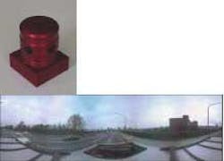
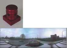
ViewPlus (Tokyo) introduced an omnidirectional digital camera that can record high-precision panoramic moving images in succession (see Fig. 1). Five charge-coupled-devices are situated in the horizontal plane with one facing upwards, capturing more than 75% of the field. The cameras are packed tightly together such that the distance between adjacent cameras is less than 20 mm. Powered by a battery, the camera can record a maximum of 30 min of moving information taken at a 15-Hz rate.
A hand-held digital high-speed camera developed by Japan Roper (Mihama-ku) was exhibited. The camera is 210 × 133 × 66 mm in size and weighs 900 g. It is designed for use in manufacturing, field services, lab experiments, and sports analysis. There are three versions with recording speeds of 250, 500 and 1000 frames/s.
The 27th Optical Symposium (Tokyo)
Engineers at Minolta (Osaka) designed a digital-camera zoom-lens unit that contains a prism. They developed this new arrangement after recognizing that the conventional configuration—in which the zoom lens unit retracts into a cavity in the main body when the power is off—puts a lower limit on camera thickness.
After evaluating the ideal lens configuration for a folding zoom-lens unit, the engineers determined that more than the conventional number of lenses would be required, spurring them to design a thin-body, low-f-stop lens. Its compactness allows very fast boot-up and shutdown of the camera. Advanced manufacturing technologies have been incorporated, including high-accuracy installation of the prism, the simultaneous alignment and installation of the aspheric lens, and a third lens incorporated to adjust the alignment. The double-concave asphere glass mold—considered difficult to manufacture—was created using a method involving liquid droplets, leading to lower cost.
Engineers at Asahi Optical (Tokyo) developed a two-sided commercial-grade aspheric lens; the lens does not require extra elements to correct chromatic aberration or coma. It is designed for use in next-generation optical disks. Next-generation optical systems aim to increase the capacity of disks fivefold by decreasing the laser wavelength and increasing the numerical aperture of the object lens.
To create such optical systems, many factors must be considered, including aberrations (spherical, coma, astigmatism, curvature of field, chromatic), materials, ease of manufacture, tolerance to manufacturing sensitivity, movement distance, environment, and compatibility with DVDs (digital versatile disks). In addition, the limited freedoms afforded by simple lenses must also be exploited. For this reason, the different aberrations in the Asahi lens had to be carefully balanced, with the chromatic aberrations reduced via high-refractive-index, low-dispersion glass mold materials.
InterOpto '02 (Mihama)
Optology Japan (Tokyo) developed an assortment of light sources that consist of optical-fiber modules using 405- to 1550-nm-emitting laser diodes and single-mode fibers. This company has established its reputation from its laser-diode and optical-fiber-system assembly techniques. By incorporating high-stability control circuits, easy-to-use, low-cost laser-diode light sources were created.
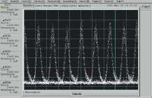
A 65-GHz oscilloscope with an electro-optic filter intended for 40-Gbit/s next-generation optical communications was displayed by Sony Techtronics (Tokyo). In addition, Ando Electric (Tokyo) exhibited an oscilloscope without an electro-optic filter intended for testing 160-Gbit/s photonic networks (see Fig. 2). The bandwidth is greater than 500 GHz.
null
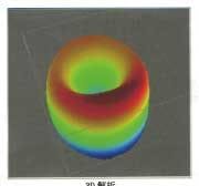
Konica (Tokyo) introduced a measurement and analysis system for 405-nm-emitting semiconductor lasers intended for next-generation high-density optical disks. A blue-laser light source interferometer, the instrument can perform high-sensitivity measurements and analysis of transmission-wavefront aberrations of optical-disk pickup lenses with numerical apertures up to 0.9 (see Fig. 3). The system can also measure and analyze the spatial characteristics of spot images.
null
Mitsui Chemical (Tokyo) exhibited an optical waveguide film made by replication. Patterns are formed into a polyimide film on top of a silicon wafer and are then coated with silicon dioxide using the spatter method, leading to a replication template. Fluorinated polymide is spin-coated onto the template; the patterns are formed by submerging it into an etching liquid, resulting in a waveguide film. Replication of features down to several dozen nanometers in size is possible. At 1550 nm, the optical loss is approximately 0.5 dB/cm. The heat-tolerance is over 300°C. The company hopes to apply this replication method to diffraction gratings, microlens arrays, and other optical systems.
Sumita Optical Glass (Saitama-Urawa) exhibited a glass-molding device for use with fluorinated precision molding glass, which can be worked at 320°C. Because the material can be worked at low temperatures, complex optical elements such as aspheric lenses that contain holograms can be created.
Courtesy O plus E magazine, Tokyo


